Failure Analysis Market by Equipment (Optical Microscope, SEM, TEM, FIB, Scanning Probe Microscope, Dual Beam), Technology (SIMS, EDX, CMP, FIB, BIM, RIE), Application, & Geography - Forecast to 2025


The Failure Analysis Market is projected to USD 5.9 Billion by 2025 from USD 4.7 billion in 2022 at a CAGR of 8.3% during the forecast period. It was observed that the growth rate was 3.91% from 2021 to 2022. Focused Ion Beam Equipment segment is expected to grow at a highest CAGR of 6.13%.
Failure analysis equipment is responsible for animating and analyzing the root cause of a failure of a product, device, or system. The failure analysis market report covers several types of failure analysis equipment such as an optical microscope, scanning probe microscope, Transmission Electron Microscope (TEM), Scanning Electron Microscope (SEM), Focused Ion Beam (FIB), and dual beam system.

Failure Analysis Equipment Market Forecast to 2025
To know about the assumptions considered for the study, Request for Free Sample Report
Failure analysis is a process that includes data collection and analysis for failure determination. Detail information, that is, how the component was procured, how it was stored before delivery, how it was handled, its location in the circuit (if mounted), how it was biased, and for how long, environmental conditions, and failure mode or degraded performance, is crucial to avoid any unprecedented damage. For instance, chips used in semiconductor devices are becoming highly integrated, and products with advanced functions have been introduced in recent years, such as multiple chips mounted in a single package. As a result, manufacturing processes are becoming more miniaturized and complex, and failure causes and mechanisms are also diversifying and becoming more complex. When manufacturing semiconductors, consistent quality and reliability must be built in from the development stage to the manufacturing stage to prevent semiconductor devices from failing and underperforming.
There are several technologies used for failure analysis. The prominent technologies used are Secondary Ion Mass Spectroscopy (SIMS), Energy Dispersive X-ray Spectroscopy (EDX), Chemical Mechanical Planarization (CMP), Focused Ion Beam (FIB), Broad Ion Milling (BIM), Reactive Ion
Etching (RIE).
Failure analysis Market Dynamics:
Driver: Imposition of safety rules and regulations by governments and international bodies
Failure Analysis techniques are used to identify defects and flaws in existing equipment and in the latest and advanced equipment/devices used across various industries. Strict product usage specifications, government safety regulations, and stringent quality control requirements are boosting the demand for failure analysis equipment. Different countries have regulatory bodies to control, develop, and publish technical industrial standards. For instance, the American Society for Nondestructive Testing (ASNT) is a member-based, non-profit professional society engaged in providing NDT-related reference material, NDT training certification documents, and conducting technical conferences.
Earlier examples of infrastructure failures, such as leakages in nuclear refineries, pipeline explosions, and refinery blasts, have impelled governments to impose stringent safety regulations, resulting in an increasing demand for failure analysis equipment. Regulatory approval plays a crucial role in the launch of a new device or instrument in the market. According to the Code of Federal Regulation 21 (CFR 21) LIS FDA, microscopes are categorized as Class I medical devices. If a device is not labeled or otherwise represented as sterile, it is exempt from the Current Good Manufacturing Practice (cGMP) regulations. These devices are also exempt from premarket notification procedures and can be launched into the market quickly.
Restraint: High ownership and maintenance cost
There has been a shift in the usage patterns of microscopes. Conventional microscopes are gradually losing their market to high-end microscopes such as electron microscopes, scanning probe microscopes, and digital microscopes due to their advanced features, higher resolution, and magnification power. However, these microscopes cost between USD 25,000 to USD 2 million, which is a major factor limiting their adoption in hospitals, pathological laboratories, and small-scale industries. Also, there are recurrent expenses in the form of maintenance costs of microscopes, which ultimately drive the overall cost of ownership. For instance, the maintenance cost of a transmission electron microscope is between USD 15,000–USD 100,000 per year. The high cost has left users reliant on government and private research funding, which is restricting market growth to a certain extent.
Opportunity: Integration of microscopy with spectroscopy
The integration of microscopy with spectroscopy is expected to present major opportunities to research communities due to its wide variety of applications. For instance, combining Raman spectroscopy with atomic force microscopy or optical microscopy provides detailed information about nanoscale properties and composition. Other benefits offered by these combined techniques include precise alignment of the sample, optical signal transfer from the microscope to the spectrometer, and precise focus of the excitation light at the detection point. The high potential of combining microscopy technologies led to developments such as the introduction of the DXR2 Raman Imaging Microscope by Thermo Fisher Scientific. This instrument consists of an optical microscope integrated with a Raman spectrometer to obtain both traditional optical and spectrochemical images.
Challenge: Dearth of skilled professionals
Physicists and laboratory technicians can efficiently operate standard compound microscopes. However, with the development of advanced microscopes, the requirement for skilled personnel has increased. For example, atomic force scanning tunneling microscopes—widely used in nanotechnology—require physicists or technicians to have thorough interdisciplinary knowledge in the field of surface physics and surface analyses to study the characterization of biological and chemical compounds at the atomic or molecular level. The complexity of advanced microscopes makes the dearth of skilled professionals a key challenge to their use and adoption.
Failure analysis Market Segment Insights:

Failure analysis market for focused ion beam (FIB) systems is expected to grow at the highest CAGR during the forecast period
The Focused Ion Beam (FIB) market is expected to grow at the highest CAGR during the forecast period. FIBS are primarily used for semiconductor manufacturing. The development of commercially focused FIBS has led to their increased applications in the field of material sciences. In addition to circuit editing and Transmission Electron Microscopy (TEM) sample preparation, FIBs can now be used for microstructural analysis and prototyping nanomachining. The fastest growth of this segment can be attributed to the growing adoption of FIB systems in material science and bioscience applications.
The failure analysis market for Energy Dispersive X-Ray Spectroscopy (EDX) to hold the largest share during the forecast period
Energy Dispersive X-ray Spectroscopy (EDX or EDS) is an analytical capability that can be coupled with several applications, including Scanning Electron Microscope (SEM), Transmission Electron Microscope (TEM), and Scanning Transmission Electron Microscopy (STEM). EDX, when combined with these imaging tools, can provide elemental analysis on areas as small as nanometers in diameter. In a multi-technique approach, EDX becomes very powerful, particularly in contamination analysis and industrial forensic science investigations.
Failure analysis market for semiconductors and electronics to hold the largest share during the forecast period.
The growing demand for miniature transistor chips, nanoelectronics, quantum dots, and optoelectronics is driving the market for failure analysis in the semiconductor industry. The electronics & semiconductor industry is one of the growing sectors globally, owing to the increased adoption of robotics and automation to produce electronic devices. The electronics & semiconductor industry requires high-density, integrated, and miniaturized devices. These requirements have led to the development of 3D Integrated Circuits (ICs) that make it possible to incorporate extensive functionalities into fast, small, and low-power-consumption devices. However, these dense ICs require sophisticated development, prototyping, inspection, and failure analysis tools.
Regional Insights:
The Asia Pacific region is projected to grow at the highest CAGR during the forecast period
The mass production of electronic products such as smartphones, tablets, sensors, industrial equipment, wearables, and white goods in China and Taiwan is expected to accelerate the growth of the regional failure analysis market. Japan is the largest market for microscopy equipment in the Asia Pacific region. Major market players such as Nikon, JEOL Ltd., Olympus, and Hitachi High-Technologies are headquartered in Japan. They have a strong customer base in the country, including several large research institutes and pharmaceutical & biotechnology companies. China's manufacturing sector is using industrial robots to automate and modernize various manufacturing processes. This trend has led to the requirement for monitoring device failure, thus offering new growth opportunities for the failure analysis market in the country.

Failure Analysis Equipment Market by Region
To know about the assumptions considered for the study, download the pdf brochure
The North America region is expected to hold the largest share of the market during the forecast period
Thermo Fisher Scientific Inc. (US), Motion X Corporation (US), FEI Company (US), and EAG Inc. (US) are some of the key manufacturers of failure analysis equipment in the North American region. The increase in the number of laboratories adopting FIB technology for their research work and the presence of key players involved in the manufacturing, distribution, and servicing of FIB systems are driving the growth of the failure analysis market in North America. The US and Canada are the top countries of the region that are expected to contribute to the North American failure analysis market. The US is expected to contribute the maximum share to the failure analysis market in North America during the forecast period, owing to the technological advancements taking place in methods used for the analysis of semiconductor raw materials as well as the willingness of manufacturers of semiconductor components to carry out innovations in their products and adopt new technologies.
Failure Analysis Market Key Players:
Some of the leading players in this market are Thermo Fisher Scientific, Inc. (US), Hitachi High-Technologies Corporation (Japan), Carl Zeiss (Germany), JOEL, Ltd. (Japan), TESCAN OSRAY HOLDING (Czech Republic), Bruker (US), Intertek Group Plc (UK), Nikon Metrology (Belgium), Semilab (Hungary), A&D Company, Ltd. (Japan), Nanosurf AG (Switzerland), HORIBA, Ltd. (Japan), Leica Microsystems GmbH (Germany), Veeco Instruments (US), Oxford Instruments (UK), Eurofins Scientific (Luxembourg), Olympus Corporation (Japan). These players have adopted various growth strategies, such as new product launches, acquisitions, and partnerships further to expand their presence in the failure analysis market.
Hitachi High-Technologies Corporation (Japan) develops, manufactures, markets, and provides service support to electronic and electrical equipment and systems. Hitachi High-Technologies Corporation is among the key players in the failure analysis market due to its continuous focus on electronic device systems as well as science & medical systems. The company has focused on technology development to spur business expansion in the failure analysis equipment industry. Major investments in the semiconductor industry across the Asia Pacific region will drive revenue growth for the Hitachi High-Tech Group.
Thermo Fisher Scientific, Inc. (US) focuses on designing, manufacturing, and supplying analytical instruments, laboratory equipment, diagnostic products, software, and services for research, clinical, and industrial applications. Thermo Fisher Scientific’s microscopes business unit falls under a prominent subsidiary named FEI Company, which operates under Thermo Fisher’s Analytical Instruments business segment. Thermo Fisher offers electron microscopes, ion-beam microscopes, FTIR-Raman microscopes, accessories, and software. The firm’s versatile, high-performance scanning electron microscopes are used for the characterization of a broad range of materials, including nanoparticles, metals, and composites & coatings.The company focuses on the expansion of its system business, to date, more than 2,000 Thermo Scientific systems have been installed across the globe.
Failure Analysis Market Report Scope:
|
Report Attributes |
Details |
|
Market Size Value in 2020 |
USD 3.9 Billion |
| Revenue Forecast in 2025 | USD 5.9 Billion |
| Growth Rate | 8.3% |
| Base Year Considered | 2019 |
| Historical Data Available for Years | 2017–2025 |
|
Forecast Period |
2020–2025 |
|
Segments Covered |
|
|
Region Covered |
|
| Market Leaders |
|
| Top Companies in North America |
|
| Key Market Driver | Imposition of safety rules and regulations by governments and international bodies |
| Key Market Opportunity | Integration of microscopy with spectroscopy |
| Largest Growing Region | Asia Pacific |
| Largest Market Share Segment | Energy Dispersive X-Ray Spectroscopy (EDX) Segment |
| Highest CAGR Segment | Focused ion beam (FIB) systems Segment |
| Largest Application Market Share | Semiconductors and Electronics Application |
This report categorizes the failure analysis based on equipment, technology, application, and geography.
Failure Analysis Market, by Equipment
- Optical Microscope
- Scanning Electron Microscope (SEM)
- Transmission Electron Microscope (TEM)
- Scanning Probe Microscope
- Focused Ion Beam System (FIB)
- Dual-Beam System (FIB-SEM)
- Others (X-ray microscopes, Raman microscopes, and Scanning Acoustic Microscopes)
Failure Analysis Market, by Technology
- Energy Dispersive X-Ray Spectroscopy (EDX)
- Secondary Ion Mass Spectrometry (SIMS)
- Focused Ion Beam (FIB)
- Broad Ion Milling (BIM)
- Relative Ion Etching (RIE)
- Scanning Probe Microscopy (SPM)
- Others (Chemical Mechanical Planarization (CMP) and X-ray Photoelectron Spectroscopy (XPS))
Failure Analysis Market, by Application
- Electronics & Semiconductor
- Industrial Science
- Material Science
- Bioscience
Failure Analysis Market, by Geography
-
North America
- US
- Canada
- Mexico
-
Europe
- UK
- Germany
- France
- Rest of Europe
-
Asia Pacific
- China
- Japan
- South Korea
- India
- Rest of Asia Pacific
-
RoW
- Middle East and Africa
- South America
Failure Analysis Equipment Market Highlights:

What is new?
- Use of focused ion beam systems to study biological samples and biomaterials
Initially, FIB systems were restricted to the electronics & semiconductor and the material sciences verticals only. Presently, they are evolving as powerful tools for the ultrastructural and nanoscale cellular imaging of biological samples and biomaterials (materials that associate immediately with the living tissues without causing any adverse immune rejection reaction). Earlier, confocal light microscopy, in combination with the traditional fluorescent labeling technique, was used by biologists and life scientists for a detailed study of the biological structures of tissues and cells. However, with the advent of FIB systems, they are being preferred over traditional techniques as it is easy to obtain information from these systems at small scales. FIB systems can be coupled with complementary cryogenic, dual-beam SEM, environmental SEM, and energy-dispersive X-ray spectroscopy (EDX) tools to analyze biomaterials and cells as well as their interfaces for TEM sample preparation by imaging them.
- Addition/refinement in segmentation–Increase in depth or width of segmentation of the market.
-
Failure analysis Market, by Techniques
- Destructive Physical Analysis (DPA)
- fault tree analysis (FTA)
- Common Mode Failure Analysis
- Failure Modes and Effects Analysis (FMEA)
- Sneak Circuit Analysis (SCA)
- Coverage of new market players and change in the market share of existing players of the failure analysis market.
Company profiles: Company profiles give a glimpse of the key players in the market with respect to their business overviews, financials, product offerings, recent developments undertaken by them, and MnM view. In the new edition of the report, we have a total of 25 players (10 major and 15 Other key companies).
- Updated financial information and product portfolios of players operating in the failure analysis market.
Newer and improved representation of financial information: The latest edition of the report provides updated financial information in the context of the failure analysis market till 2021/2022 for each listed company in the graphical representation in a single diagram (instead of multiple tables). This would help to quickly analyze the present status of profiled companies in terms of their financial strength, profitability, critical revenue-generating region/country, business segment focus in terms of the highest revenue-generating segment, and investment in research and development activities.
- Updated market developments of the profiled players.
Recent Developments: Updated market developments such as contracts, joint ventures, partnerships & agreements, acquisitions, new product launches, investments, and funding, have been mapped for the years 2019 to 2022.
Recent Developments
- In December 2021, Hamamatsu Photonics developed a new semiconductor failure analysis system called the “PHEMOS-X C15765-01” in just a single unit, which utilizes visible to near-infrared light to analyze semiconductor defects.
- In August 2021, TESCAN ORSAY HOLDING a.s. launched their Large Volume Workflow to support semiconductor, automotive, and aerospace industries and their related research fields that are now experiencing an increasing need for large volume material removal to reach regions of interest faster for failure and defect root-cause analyses.
- In August 2020, Thermo Fisher Scientific released the nProber IV nanoprober platform, a fault isolation system used by semiconductor fabs to precisely locate and characterise nanometer-scale electrical faults that impact device performance and reliability.
- Key Benefits of the Report/Reason to Buy:
-
Target Audience:
Frequently Asked Questions (FAQ):
What is the current size of the failure analysis market?
The failure analysis market is projected to grow from USD 3.9 billion in 2020 to USD 5.9 Billion by 2025, at a CAGR of 8.3% from 2020 to 2025.
Who are the key players in the failure analysis market?
Some of the leading players in this market are Thermo Fisher Scientific, Inc. (US), Hitachi High-Technologies Corporation (Japan), Carl Zeiss (Germany), JOEL, Ltd. (Japan), TESCAN OSRAY HOLDING (Czech Republic), Bruker (US), Intertek Group Plc (UK), Nikon Metrology (Belgium).
What are the opportunities for new market entrants?
The increasing demand in developing countries, growing integration of microscopy with spectroscopy, and rising usage of focused ion beam systems to study biological samples and biomaterials act as growth opportunities for the failure analysis market.
Which application is expected to dominate the failure analysis market?
The failure analysis market for the electronics & semiconductor segment will likely account for the largest share during the forecast period. The growing demand for miniature transistor chips, nanoelectronics, quantum dots, and optoelectronics is driving the need for failure analysis in the semiconductors industry.
Which region is expected to lead the failure analysis market?
Asia Pacific is the leading market for failure analysis and is expected to witness significant growth in the coming years. The failure analysis market in Asia Pacific is growing at a rapid rate owing to the proliferation of Internet services and rapid Internet penetration.
To speak to our analyst for a discussion on the above findings, click Speak to Analyst
TABLE OF CONTENTS
1 INTRODUCTION (Page No. - 19)
1.1 STUDY OBJECTIVES
1.2 MARKET DEFINITION AND SCOPE
1.2.1 INCLUSIONS AND EXCLUSIONS
1.3 STUDY SCOPE
1.3.1 MARKETS COVERED
1.3.2 GEOGRAPHIC SCOPE
1.4 YEARS CONSIDERED
1.5 CURRENCY
1.6 LIMITATIONS
1.7 STAKEHOLDERS
1.8 SUMMARY OF CHANGES
2 RESEARCH METHODOLOGY (Page No. - 23)
2.1 RESEARCH DATA
2.1.1 SECONDARY DATA
2.1.1.1 Secondary sources
2.1.2 PRIMARY DATA
2.1.2.1 Primary sources
2.1.2.2 Breakdown of primary interviews
2.1.3 SECONDARY AND PRIMARY RESEARCH
2.2 MARKET SIZE ESTIMATION
2.2.1 BOTTOM-UP APPROACH
2.2.1.1 Approach for capturing market size using bottom-up analysis (demand side)
2.2.2 TOP-DOWN APPROACH
2.2.2.1 Approach for capturing market share using top-down analysis (supply side)
2.3 DATA TRIANGULATION
2.4 ASSUMPTIONS
3 EXECUTIVE SUMMARY (Page No. - 32)
4 PREMIUM INSIGHTS (Page No. - 36)
4.1 ATTRACTIVE OPPORTUNITIES IN THE FAILURE ANALYSIS MARKET
4.2 MARKET IN ASIA PACIFIC, BY EQUIPMENT AND APPLICATION
4.3 MARKET, BY TECHNOLOGY
4.4 MARKET, BY GEOGRAPHY
5 MARKET OVERVIEW (Page No. - 39)
5.1 INTRODUCTION
5.2 MARKET DYNAMICS
5.2.1 DRIVERS
5.2.1.1 Imposition of safety rules and regulations by governments and international bodies
5.2.1.2 Rise in demand for failure analysis from the electronics & semiconductor industry
5.2.1.3 Technological advancements in microscopes
5.2.1.4 Rising focus on nanotechnology and regenerative medicine
5.2.2 RESTRAINTS
5.2.2.1 High ownership and maintenance cost
5.2.3 OPPORTUNITIES
5.2.3.1 Increasing demand for failure analysis in developing countries
5.2.3.2 Integration of microscopy with spectroscopy
5.2.3.3 Use of focused ion beam systems to study biological samples and biomaterials
5.2.4 CHALLENGES
5.2.4.1 Dearth of skilled professionals
5.3 VALUE CHAIN ANALYSIS
5.4 COVID-19 IMPACT ON FAILURE ANALYSIS MARKET
6 FAILURE ANALYSIS MARKET, BY EQUIPMENT (Page No. - 48)
6.1 INTRODUCTION
6.2 OPTICAL MICROSCOPE
6.2.1 HIGH ADOPTION OF OPTICAL MICROSCOPES FOR LOCATING AND IDENTIFYING EXTERNAL DEFECTS TO DRIVE THE MARKET
6.3 SCANNING ELECTRON MICROSCOPE (SEM)
6.3.1 INCREASING ADOPTION OF SCANNING ELECTRON MICROSCOPES IN VARIOUS INDUSTRIES SUCH AS MATERIAL SCIENCE AND SEMICONDUCTORS TO DRIVE THE MARKET
6.4 TRANSMISSION ELECTRON MICROSCOPE (TEM)
6.4.1 HIGH ADOPTION OF TRANSMISSION ELECTRON MICROSCOPES FOR LIFE SCIENCE, MATERIAL SCIENCE, AND METALLURGY TO DRIVE THE MARKET
6.5 SCANNING PROBE MICROSCOPE (SPM)
6.5.1 INCREASING DEMAND FOR ATOMIC FORCE MICROSCOPY FROM MINIATURE ELECTRONIC AND SEMICONDUCTOR DEVICES IS DRIVING THE MARKET
6.6 FOCUSED ION BEAM (FIB) SYSTEM
6.6.1 MARKET FOR FOCUSED ION BEAM SYSTEMS IS EXPECTED TO GROW AT THE HIGHEST CAGR DURING THE FORECAST PERIOD
6.7 DUAL BEAM SYSTEM
6.7.1 MARKET FOR DUAL BEAM SYSTEMS IS EXPECTED TO GROW AT THE SECOND HIGHEST CAGR DURING FORECAST PERIOD
6.8 OTHERS
7 FAILURE ANALYSIS MARKET, BY TECHNOLOGY (Page No. - 70)
7.1 INTRODUCTION
7.2 ENERGY DISPERSIVE X-RAY SPECTROSCOPY (EDX)
7.2.1 EDX CAN BE COUPLED WITH SEM, TEM, AND STEM TECHNOLOGIES, WHICH IS LIKELY TO DRIVE THE DEMAND FOR THIS TECHNOLOGY
7.3 SECONDARY ION MASS SPECTROSCOPY (SIMS)
7.3.1 WIDE ADOPTION OF SIMS IN MATERIAL SCIENCE APPLICATIONS IS LIKELY TO DRIVE THE SEGMENT
7.4 FOCUSED ION BEAM (FIB)
7.4.1 DEMAND FROM NANOFABRICATION AND MICROMACHINING-RELATED APPLICATIONS IS LIKELY TO DRIVE THE FIB SEGMENT
7.5 BROAD ION MILLING (BIM)
7.5.1 HIGH-QUALITY TEM SAMPLING ABILITIES ARE LIKELY TO DRIVE THE DEMAND FOR BIM TECHNOLOGY
7.6 REACTIVE ION ETCHING (RIE)
7.6.1 INCREASED PRODUCT DENSITY, IMPROVED YIELDS, AND TIGHTER TOLERANCES FROM THE ELECTRONICS INDUSTRY ARE LIKELY TO BOOST THE DEMAND FOR REACTIVE ION ETCHING
7.7 SCANNING PROBE MICROSCOPY (SPM)
7.7.1 INCREASED DEMAND FROM SEMICONDUCTORS, MATERIAL SCIENCE, ELECTRONICS, AND NANOTECHNOLOGY FOR TOPOGRAPHIC ANALYSIS TO BOOST THE SPM SEGMENT
7.8 OTHERS
7.9 OVERVIEW OF FAILURE ANALYSIS TECHNIQUES (QUALITATIVE)
7.9.1 DESTRUCTIVE PHYSICAL ANALYSIS (DPA)
7.9.2 FAULT TREE ANALYSIS (FTA)
7.9.3 COMMON-MODE FAILURE ANALYSIS
7.9.4 FAILURE MODES AND EFFECTS ANALYSIS (FMEA)
7.9.5 SNEAK CIRCUIT ANALYSIS
8 FAILURE ANALYSIS MARKET, BY APPLICATION (Page No. - 76)
8.1 INTRODUCTION
8.2 ELECTRONICS & SEMICONDUCTOR
8.2.1 SEMICONDUCTOR MANUFACTURING
8.2.1.1 Increasingly complex circuitry leads to the requirement for failure analysis of different electronic components and devices
8.2.2 MEMS AND THIN FILM PRODUCTION
8.2.2.1 Focused ion beam systems are used for failure analysis of MEMS and identification of root causes of these failures
8.3 INDUSTRIAL SCIENCE
8.3.1 OIL & GAS
8.3.1.1 FIB-SEM systems provide new insights related to the reservoir flow control mechanism for the oil & gas vertical
8.3.2 AUTOMOTIVE AND AEROSPACE
8.3.2.1 Increased demand for electronic systems in autonomous and driverless cars is likely to drive the market for the automotive sector
8.3.3 CHEMICALS
8.3.3.1 Dual beam microscopes carry out the high-fidelity 3D characterization of crystallography, morphology, and chemistry of micro- and submicro-sized features of different components
8.3.4 POWER GENERATION
8.3.4.1 Scanning electron microscope high-resolution imaging is used for the analysis of microstructural changes in power plants
8.4 MATERIAL SCIENCE
8.4.1 METALS AND MINING
8.4.1.1 High adoption of scanning electron microscopes, transmission electron microscopes, and focused ion beam systems to gain an improved understanding of the physical properties of metals
and alloys 83
8.4.2 PAPER AND FIBER MATERIALS
8.4.2.1 Focused ion beam systems provide failure analysis of paper and fiber materials
8.4.3 CERAMIC AND GLASS
8.4.3.1 Focused ion beam systems provide nanofabrication, milling, and imaging of ceramics and glass
8.4.4 POLYMERS
8.4.4.1 High adoption of scanning electron microscopes in modern material science investigations into polymers and plastics is driving the segment
8.4.5 NANOFABRICATION
8.4.5.1 Focused ion beam offers patterning solutions for nanofabrication
8.5 BIOSCIENCE
8.5.1 CELLULAR BIOLOGY
8.5.1.1 Examination of 3D cell and tissue architecture using SEM and TEM is boosting the segment
8.5.2 STRUCTURAL BIOLOGY
8.5.2.1 FIB-SEM systems are being used extensively for studying structural biology
8.5.3 BIOMEDICAL ENGINEERING
8.5.3.1 FIB and TEM systems are aiding research activities for biotechnology and implantable biomedical devices
8.5.4 NEUROSCIENCE
8.5.4.1 3D biological samples imaging is done through FIB-SEM systems
9 FAILURE ANALYSIS MARKET, BY GEOGRAPHY (Page No. - 89)
9.1 INTRODUCTION
9.2 NORTH AMERICA
9.2.1 US
9.2.1.1 Increasing R&D and growing commercialization of nanotechnology-based products are driving the demand for failure analysis in the US
9.2.2 CANADA
9.2.2.1 Initiatives by different institutions, research laboratories, and companies in Canada are driving the market
9.2.3 MEXICO
9.2.3.1 Increasing adoption of advanced technologies in electronics & semiconductor and material science verticals is fueling the demand for failure analysis equipment in Mexico
9.3 EUROPE
9.3.1 GERMANY
9.3.1.1 Favorable funding scenario for R&D in microscopy, growth in the biotechnology industry, and rise in focus on nanotechnology are driving the failure analysis market in Germany
9.3.2 UK
9.3.2.1 Increase in R&D investments in biotechnology, nanotechnology, and life sciences is expected to surge the demand for failure analysis equipment in the UK
9.3.3 FRANCE
9.3.3.1 Growing biotechnology industry is likely to propel the market growth in France
9.3.4 REST OF EUROPE
9.4 ASIA PACIFIC
9.4.1 JAPAN
9.4.1.1 Consistent and increased investments in R&D activities by key players are likely to drive the market in Japan
9.4.2 CHINA
9.4.2.1 Growing demand for failure analysis equipment from electronics & semiconductor, automotive, and other consumer industries is likely to drive the market
9.4.3 SOUTH KOREA
9.4.3.1 Increased adoption of FIB and FIB-SEM systems and solutions in laboratories, universities, and manufacturing companies is contributing to the growth of the market in South Korea
9.4.4 INDIA
9.4.4.1 Increase in government initiatives to support the growth of the electronics & semiconductor industry is likely to drive the market in India
9.4.5 REST OF ASIA PACIFIC
9.5 REST OF THE WORLD (ROW)
9.5.1 MIDDLE EAST & AFRICA
9.5.1.1 Increase in demand for failure analysis equipment from consumer electronics, automotive, and aerospace & defense industries is likely to drive the market in the Middle East & Africa
9.5.2 SOUTH AMERICA
9.5.2.1 Increase in investments in bioscience research is likely to drive the market in South America
10 COMPETITIVE LANDSCAPE (Page No. - 117)
10.1 OVERVIEW
10.2 MARKET PLAYER RANKING ANALYSIS
10.3 COMPETITIVE LEADERSHIP MAPPING
10.3.1 VISIONARY LEADERS
10.3.2 INNOVATORS
10.3.3 DYNAMIC DIFFERENTIATORS
10.3.4 EMERGING COMPANIES
10.4 COMPETITIVE SCENARIO
10.4.1 PRODUCT LAUNCHES AND DEVELOPMENTS
10.4.2 ACQUISITIONS, PARTNERSHIPS, AGREEMENTS, AND COLLABORATIONS
11 COMPANY PROFILES (Page No. - 124)
11.1 KEY PLAYERS
(Business Overview, Products Offered, Recent Developments, SWOT Analysis, and MnM View)*
11.1.1 HITACHI HIGH-TECHNOLOGIES CORPORATION
11.1.2 THERMO FISHER SCIENTIFIC, INC.
11.1.3 CARL ZEISS
11.1.4 JEOL LTD.
11.1.5 TESCAN OSRAY HOLDING
11.1.6 BRUKER
11.1.7 HORIBA, LTD.
11.1.8 SEMILAB
11.1.9 A&D COMPANY LTD.
11.1.10 MOTION X CORPORATION
* Business Overview, Products Offered, Recent Developments, SWOT Analysis, and MnM View might not be captured in case of unlisted companies.
11.2 RIGHT TO WIN
11.3 OTHER KEY PLAYERS
11.3.1 EUROFINS SCIENTIFIC
11.3.2 INTERTEK GROUP PLC
11.3.3 OXFORD INSTRUMENTS
11.3.4 RAITH GMBH
11.3.5 LEICA MICROSYSTEMS
11.3.6 VEECO INSTRUMENTS
11.3.7 ACCU-SCOPE
11.3.8 MEIJI TECHNO CO.
11.3.9 FIBICS
11.3.10 APPLIED BEAMS
12 APPENDIX (Page No. - 157)
12.1 DISCUSSION GUIDE
12.2 KNOWLEDGE STORE: MARKETSANDMARKETS’ SUBSCRIPTION PORTAL
12.3 AVAILABLE CUSTOMIZATIONS
12.4 RELATED REPORTS
12.5 AUTHOR DETAILS
LIST OF TABLES (100 TABLES)
TABLE 1 FAILURE ANALYSIS MARKET, BY EQUIPMENT, 2017–2025 (USD MILLION)
TABLE 2 MARKET FOR OPTICAL MICROSCOPE, BY APPLICATION, 2017–2025 (USD MILLION)
TABLE 3 MARKET FOR OPTICAL MICROSCOPE, BY REGION, 2017–2025 (USD MILLION)
TABLE 4 MARKET FOR OPTICAL MICROSCOPE IN NORTH AMERICA, BY COUNTRY, 2017–2025 (USD MILLION)
TABLE 5 MARKET FOR OPTICAL MICROSCOPE IN EUROPE, BY COUNTRY, 2017–2025 (USD MILLION)
TABLE 6 MARKET FOR OPTICAL MICROSCOPE IN ASIA PACIFIC, BY COUNTRY, 2017–2025 (USD MILLION)
TABLE 7 MARKET FOR OPTICAL MICROSCOPE IN ROW, BY REGION, 2017–2025 (USD MILLION)
TABLE 8 MARKET FOR SCANNING ELECTRON MICROSCOPE, BY APPLICATION, 2017–2025 (USD MILLION)
TABLE 9 MARKET FOR SCANNING ELECTRON MICROSCOPE, BY REGION, 2017–2025 (USD MILLION)
TABLE 10 MARKET FOR SCANNING ELECTRON MICROSCOPE IN NORTH AMERICA, BY COUNTRY, 2017–2025 (USD MILLION)
TABLE 11 MARKET FOR SCANNING ELECTRON MICROSCOPE IN EUROPE, BY COUNTRY, 2017–2025 (USD MILLION)
TABLE 12 MARKET FOR SCANNING ELECTRON MICROSCOPE IN ASIA PACIFIC, BY COUNTRY, 2017–2025 (USD MILLION)
TABLE 13 MARKET FOR SCANNING ELECTRON MICROSCOPE IN ROW, BY REGION, 2017–2025 (USD MILLION)
TABLE 14 MARKET FOR TRANSMISSION ELECTRON MICROSCOPE, BY APPLICATION, 2017–2025 (USD MILLION)
TABLE 15 MARKET FOR TRANSMISSION ELECTRON MICROSCOPE, BY REGION, 2017–2025 (USD MILLION)
TABLE 16 MARKET FOR TRANSMISSION ELECTRON MICROSCOPE IN NORTH AMERICA, BY COUNTRY, 2017–2025 (USD MILLION)
TABLE 17 MARKET FOR TRANSMISSION ELECTRON MICROSCOPE IN EUROPE, BY COUNTRY, 2017–2025 (USD MILLION)
TABLE 18 MARKET FOR TRANSMISSION ELECTRON MICROSCOPE IN ASIA PACIFIC, BY COUNTRY, 2017–2025 (USD MILLION)
TABLE 19 MARKET FOR TRANSMISSION ELECTRON MICROSCOPE IN ROW, BY REGION, 2017–2025 (USD MILLION)
TABLE 20 TYPES OF SCANNING PROBE MICROSCOPE (SPM)
TABLE 21 MARKET FOR SCANNING PROBE MICROSCOPE, BY APPLICATION, 2017–2025 (USD MILLION)
TABLE 22 MARKET FOR SCANNING PROBE MICROSCOPE, BY REGION, 2017–2025 (USD MILLION)
TABLE 23 MARKET FOR SCANNING PROBE MICROSCOPE IN NORTH AMERICA, BY COUNTRY, 2017–2025 (USD MILLION)
TABLE 24 MARKET FOR SCANNING PROBE MICROSCOPE IN EUROPE, BY COUNTRY, 2017–2025 (USD MILLION)
TABLE 25 MARKET FOR SCANNING PROBE MICROSCOPE IN ASIA PACIFIC, BY COUNTRY, 2017–2025 (USD MILLION)
TABLE 26 MARKET FOR SCANNING PROBE MICROSCOPE IN ROW, BY REGION, 2017–2025 (USD MILLION)
TABLE 27 MARKET FOR FOCUSED ION BEAM SYSTEM, BY APPLICATION, 2017–2025 (USD MILLION)
TABLE 28 MARKET FOR FOCUSED ION BEAM SYSTEM, BY REGION, 2017–2025 (USD MILLION)
TABLE 29 MARKET FOR FOCUSED ION BEAM SYSTEM IN NORTH AMERICA, BY COUNTRY, 2017–2025 (USD MILLION)
TABLE 30 MARKET FOR FOCUSED ION BEAM SYSTEM IN EUROPE, BY COUNTRY, 2017–2025 (USD MILLION)
TABLE 31 MARKET FOR FOCUSED ION BEAM SYSTEM IN ASIA PACIFIC, BY COUNTRY, 2017–2025 (USD MILLION)
TABLE 32 MARKET FOR FOCUSED ION BEAM SYSTEM IN ROW, BY REGION, 2017–2025 (USD MILLION)
TABLE 33 MARKET FOR DUAL BEAM SYSTEM, BY APPLICATION, 2017–2025 (USD MILLION)
TABLE 34 MARKET FOR DUAL BEAM SYSTEM, BY REGION, 2017–2025 (USD MILLION)
TABLE 35 MARKET FOR DUAL BEAM SYSTEM IN NORTH AMERICA, BY COUNTRY, 2017–2025 (USD MILLION)
TABLE 36 MARKET FOR DUAL BEAM SYSTEM IN EUROPE, BY COUNTRY, 2017–2025 (USD MILLION)
TABLE 37 MARKET FOR DUAL BEAM SYSTEM IN ASIA PACIFIC, BY COUNTRY, 2017–2025 (USD MILLION)
TABLE 38 MARKET FOR DUAL BEAM SYSTEM IN ROW, BY REGION, 2017–2025 (USD MILLION)
TABLE 39 MARKET FOR OTHERS, BY APPLICATION, 2017–2025 (USD MILLION)
TABLE 40 MARKET FOR OTHERS, BY REGION, 2017–2025 (USD MILLION)
TABLE 41 MARKET FOR OTHERS IN NORTH AMERICA, BY COUNTRY, 2017–2025 (USD MILLION)
TABLE 42 MARKET FOR OTHERS IN EUROPE, BY COUNTRY, 2017–2025 (USD MILLION)
TABLE 43 MARKET FOR OTHERS IN ASIA PACIFIC, BY COUNTRY, 2017–2025 (USD MILLION)
TABLE 44 MARKET FOR OTHERS IN ROW, BY REGION, 2017–2025 (USD MILLION)
TABLE 45 FAILURE ANALYSIS MARKET, BY TECHNOLOGY, 2017–2025 (USD MILLION)
TABLE 46 MARKET, BY APPLICATION, 2017–2025 (USD MILLION)
TABLE 47 ELECTRONICS & SEMICONDUCTOR FAILURE ANALYSIS TECHNIQUES
TABLE 48 MARKET FOR ELECTRONICS & SEMICONDUCTOR, BY EQUIPMENT, 2017–2025 (USD MILLION)
TABLE 49 MARKET FOR ELECTRONICS & SEMICONDUCTOR, BY REGION, 2017–2025 (USD MILLION)
TABLE 50 MARKET FOR INDUSTRIAL SCIENCE, BY EQUIPMENT, 2017–2025 (USD MILLION)
TABLE 51 MARKET FOR INDUSTRIAL SCIENCE, BY REGION, 2017–2025 (USD MILLION)
TABLE 52 MARKET FOR MATERIAL SCIENCE, BY EQUIPMENT, 2017–2025 (USD MILLION)
TABLE 53 MARKET FOR MATERIAL SCIENCE, BY REGION, 2017–2025 (USD MILLION)
TABLE 54 MARKET FOR BIOSCIENCE, BY EQUIPMENT, 2017–2025 (USD MILLION)
TABLE 55 MARKET FOR BIOSCIENCE, BY REGION, 2017–2025 (USD MILLION)
TABLE 56 MARKET, BY REGION, 2017–2025 (USD MILLION)
TABLE 57 MARKET IN NORTH AMERICA, BY EQUIPMENT, 2017–2025 (USD MILLION)
TABLE 58 MARKET IN NORTH AMERICA, BY APPLICATION, 2017–2025 (USD MILLION)
TABLE 59 MARKET IN NORTH AMERICA, BY COUNTRY, 2017–2025 (USD MILLION)
TABLE 60 MARKET IN US, BY APPLICATION, 2017–2025 (USD MILLION)
TABLE 61 MARKET IN CANADA, BY APPLICATION, 2017–2025 (USD MILLION)
TABLE 62 MARKET IN MEXICO, BY APPLICATION, 2017–2025 (USD MILLION)
TABLE 63 MARKET FOR ELECTRONICS & SEMICONDUCTOR IN NORTH AMERICA, BY COUNTRY, 2017–2025 (USD MILLION)
TABLE 64 MARKET FOR INDUSTRIAL SCIENCE IN NORTH AMERICA, BY COUNTRY, 2017–2025 (USD MILLION
TABLE 65 MARKET FOR MATERIAL SCIENCE IN NORTH AMERICA, BY COUNTRY, 2017–2025 (USD MILLION)
TABLE 66 MARKET FOR BIOSCIENCE IN NORTH AMERICA, BY COUNTRY, 2017–2025 (USD MILLION)
TABLE 67 MARKET IN EUROPE, BY EQUIPMENT, 2017–2025 (USD MILLION)
TABLE 68 MARKET IN EUROPE, BY APPLICATION, 2017–2025 (USD MILLION)
TABLE 69 FAILURE ANALYSIS MARKET IN EUROPE, BY COUNTRY, 2017–2025 (USD MILLION)
TABLE 70 MARKET IN GERMANY, BY APPLICATION, 2017–2025 (USD MILLION)
TABLE 71 MARKET IN UK, BY APPLICATION, 2017–2025 (USD MILLION)
TABLE 72 MARKET IN FRANCE, BY APPLICATION, 2017–2025 (USD MILLION)
TABLE 73 MARKET IN REST OF EUROPE, BY APPLICATION, 2017–2025 (USD MILLION)
TABLE 74 MARKET FOR ELECTRONICS & SEMICONDUCTOR IN EUROPE, BY COUNTRY, 2017–2025 (USD MILLION)
TABLE 75 MARKET FOR INDUSTRIAL SCIENCE IN EUROPE, BY COUNTRY, 2017–2025 (USD MILLION)
TABLE 76 MARKET FOR MATERIAL SCIENCE IN EUROPE, BY COUNTRY, 2017–2025 (USD MILLION)
TABLE 77 MARKET FOR BIOSCIENCE IN EUROPE, BY COUNTRY, 2017–2025 (USD MILLION)
TABLE 78 MARKET IN ASIA PACIFIC, BY EQUIPMENT, 2017–2025 (USD MILLION)
TABLE 79 MARKET IN ASIA PACIFIC, BY APPLICATION, 2017–2025 (USD MILLION)
TABLE 80 MARKET IN ASIA PACIFIC, BY COUNTRY, 2017–2025 (USD MILLION)
TABLE 81 MARKET IN JAPAN, BY APPLICATION, 2017–2025 (USD MILLION)
TABLE 82 MARKET IN CHINA, BY APPLICATION, 2017–2025 (USD MILLION)
TABLE 83 MARKET IN SOUTH KOREA, BY APPLICATION, 2017–2025 (USD MILLION)
TABLE 84 MARKET IN INDIA, BY APPLICATION, 2017–2025 (USD MILLION)
TABLE 85 MARKET IN REST OF ASIA PACIFIC, BY APPLICATION, 2017–2025 (USD MILLION)
TABLE 86 MARKET FOR ELECTRONICS & SEMICONDUCTOR IN ASIA PACIFIC, BY COUNTRY, 2017–2025 (USD MILLION)
TABLE 87 MARKET FOR INDUSTRIAL SCIENCE IN ASIA PACIFIC, BY COUNTRY, 2017–2025 (USD MILLION)
TABLE 88 MARKET FOR MATERIAL SCIENCE IN ASIA PACIFIC, BY COUNTRY, 2017–2025 (USD MILLION)
TABLE 89 MARKET FOR BIOSCIENCE IN ASIA PACIFIC, BY COUNTRY, 2017–2025 (USD MILLION)
TABLE 90 MARKET IN ROW, BY EQUIPMENT, 2017–2025 (USD MILLION)
TABLE 91 MARKET IN ROW, BY APPLICATION, 2017–2025 (USD MILLION)
TABLE 92 FAILURE ANALYSIS MARKET IN ROW, BY REGION, 2017–2025 (USD MILLION)
TABLE 93 MARKET IN MIDDLE EAST & AFRICA, BY APPLICATION, 2017–2025 (USD MILLION)
TABLE 94 MARKET IN SOUTH AMERICA, BY APPLICATION, 2017–2025 (USD MILLION)
TABLE 95 MARKET FOR ELECTRONICS & SEMICONDUCTOR IN ROW, BY REGION, 2017–2025 (USD MILLION)
TABLE 96 MARKET FOR INDUSTRIAL SCIENCE IN ROW, BY REGION, 2017–2025 (USD MILLION)
TABLE 97 MARKET FOR MATERIAL SCIENCE IN ROW, BY REGION, 2017–2025 (USD MILLION)
TABLE 98 MARKET FOR BIOSCIENCE IN ROW, BY REGION, 2017–2025 (USD MILLION)
TABLE 99 TOP FIVE PRODUCT LAUNCHES AND DEVELOPMENTS, JANUARY 2018–MARCH 2020
TABLE 100 TOP FIVE ACQUISITIONS, PARTNERSHIPS, AGREEMENTS, AND COLLABORATIONS, JANUARY 2018–MARCH 2020
LIST OF FIGURES (37 FIGURES)
FIGURE 1 FAILURE ANALYSIS MARKET SEGMENTATION
FIGURE 2 RESEARCH FLOW
FIGURE 3 FAILURE ANALYSIS MARKET: RESEARCH DESIGN
FIGURE 4 BOTTOM-UP APPROACH
FIGURE 5 TOP-DOWN APPROACH
FIGURE 6 DATA TRIANGULATION
FIGURE 7 MATERIAL SCIENCE SEGMENT OF THE MARKET IS PROJECTED TO GROW AT THE HIGHEST CAGR FROM 2020 TO 2025
FIGURE 8 OPTICAL MICROSCOPE TO HOLD THE LARGEST SHARE OF THE MARKET FROM 2020 TO 2025
FIGURE 9 FOCUSED ION BEAM TECHNOLOGY TO GROW AT THE HIGHEST CAGR IN THE MARKET FROM 2020 TO 2025
FIGURE 10 ASIA PACIFIC IS ESTIMATED TO ACCOUNT FOR THE LARGEST SHARE OF THE MARKET IN 2020
FIGURE 11 RISE IN DEMAND FOR FAILURE ANALYSIS FROM THE ELECTRONICS & SEMICONDUCTOR INDUSTRY AND TECHNOLOGICAL ADVANCEMENTS IN MICROSCOPES ARE DRIVING THE GROWTH OF THE MARKET FROM 2020 TO 2025
FIGURE 12 OPTICAL MICROSCOPE AND ELECTRONICS & SEMICONDUCTOR SEGMENTS TO HOLD LARGEST SHARES OF THE MARKET IN ASIA PACIFIC IN 2020
FIGURE 13 MARKET FOR FOCUSED ION BEAM TECHNOLOGY IS PROJECTED TO GROW AT THE HIGHEST CAGR FROM 2020 TO 2025
FIGURE 14 US IS ESTIMATED TO ACCOUNT FOR THE LARGEST SHARE OF THE MARKET IN 2020
FIGURE 15 FAILURE ANALYSIS MARKET: DRIVERS, RESTRAINTS, OPPORTUNITIES, AND CHALLENGES
FIGURE 16 FAILURE ANALYSIS MARKET DRIVERS AND THEIR IMPACT
FIGURE 17 FAILURE ANALYSIS MARKET RESTRAINT AND ITS IMPACT
FIGURE 18 FAILURE ANALYSIS MARKET OPPORTUNITIES AND THEIR IMPACT
FIGURE 19 FAILURE ANALYSIS MARKET CHALLENGES AND THEIR IMPACT
FIGURE 20 FAILURE ANALYSIS MARKET: VALUE CHAIN ANALYSIS
FIGURE 21 OPTICAL MICROSCOPE SEGMENT IS EXPECTED TO ACCOUNT FOR THE LARGEST SHARE OF THE MARKET DURING THE FORECAST PERIOD
FIGURE 22 ENERGY DISPERSIVE X-RAY SPECTROSCOPY (EDX) SEGMENT IS EXPECTED TO ACCOUNT FOR THE LARGEST SHARE OF THE MARKET DURING THE FORECAST PERIOD
FIGURE 23 MATERIAL SCIENCE SEGMENT IS EXPECTED TO GROW AT THE HIGHEST CAGR DURING THE FORECAST PERIOD
FIGURE 24 GEOGRAPHIC SNAPSHOT OF THE MARKET
FIGURE 25 NORTH AMERICA: GEOGRAPHIC SNAPSHOT
FIGURE 26 EUROPE: GEOGRAPHIC SNAPSHOT
FIGURE 27 ASIA PACIFIC: GEOGRAPHIC SNAPSHOT
FIGURE 28 COMPANIES ADOPTED PARTNERSHIPS, AGREEMENTS, AND COLLABORATIONS AS KEY GROWTH STRATEGIES FROM JANUARY 2018 TO MARCH 2020
FIGURE 29 TOP 5 PLAYERS IN THE FAILURE ANALYSIS MARKET, 2019
FIGURE 30 MARKET (GLOBAL) COMPETITIVE LEADERSHIP MAPPING, 2019
FIGURE 31 MARKET EVALUATION FRAMEWORK: PRODUCT LAUNCHES FUELED GROWTH AND INNOVATION DURING 2018–2019
FIGURE 32 HITACHI HIGH-TECHNOLOGIES CORPORATION: COMPANY SNAPSHOT
FIGURE 33 THERMO FISHER SCIENTIFIC, INC.: COMPANY SNAPSHOT
FIGURE 34 CARL ZEISS: COMPANY SNAPSHOT
FIGURE 35 JEOL LTD.: COMPANY SNAPSHOT
FIGURE 36 BRUKER: COMPANY SNAPSHOT
FIGURE 37 HORIBA, LTD.: COMPANY SNAPSHOT
The study involved 4 major activities in estimating the size of the failure analysis market. Exhaustive secondary research has been done to collect information on the failure analysis market. Validation of these findings, assumptions, and sizing with industry experts across value chain through primary research has been the next step. Both top-down and bottom-up approaches have been employed to estimate the complete market size. After that, market breakdown and data triangulation have been used to estimate the market size of segments and subsegments.
Secondary Research
In the secondary research, various secondary sources have been referred to for identifying and collecting information important for this study. Secondary sources include corporate filings (such as annual reports, investor presentations, and financial statements); trade, business, and professional associations; white papers, failure analysis–related journals, and certified publications; articles from recognized authors; gold and silver standard websites; directories; and databases. Few examples of secondary sources are Microscopy Society of America (MSA), European Microbeam Analysis Society (EMAS, and European Microscopy Society.
Primary Research
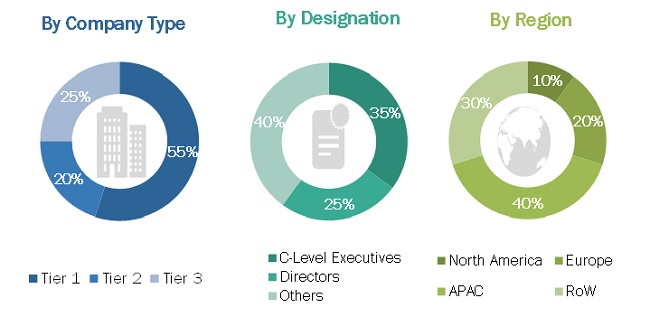
In the primary research, various primary sources from both the supply and demand sides have been interviewed to obtain the qualitative and quantitative information for this report. Primary sources from the supply side include industry experts such as CEOs, VPs, marketing directors, technology and innovation directors, and related key executives from major companies and organizations operating in the failure analysis market. Following is the breakdown of primary respondents.
To know about the assumptions considered for the study, download the pdf brochure
Market Size Estimation
Both top-down and bottom-up approaches have been used to estimate and validate the size of the failure market and its subsegments. The research methodology used to estimate the market size includes the following:
- Key players in the market have been identified through extensive secondary research
- The industry’s supply chain and market size, in terms of value, have been determined through primary and secondary research processes
- All percentage shares, splits, and breakdowns have been determined using secondary sources and verified through primary sources
Data Triangulation
After arriving at the overall market size—using the estimation processes explained above—the market has been split into several segments and subsegments. To complete the overall market engineering process and arrive at the exact statistics of each market segment and subsegment, data triangulation and market breakdown procedures have been employed, wherever applicable. The data has been triangulated by studying various factors and trends in both demand and supply sides of the failure analysis market.
Report Objectives
- To describe and forecast the failure analysis market, in terms of value, based on technology, equipment, and application
- To describe and forecast the market, in terms of value, for four major regions—North America, Europe, Asia Pacific, and the Rest of the World (RoW)
- To provide detailed information regarding factors such as drivers, restraints, opportunities, and challenges influencing the growth of the market
- To strategically analyze micromarkets1 with respect to individual growth trends, and contributions to the total market
- To profile key players and comprehensively analyze their position in terms of the market ranking and core competencies2, along with a detailed competitive landscape of the market
- To analyze the competitive growth strategies—collaborations, agreements, partnerships, acquisitions, product launches and developments, research and development (R&D) activities—adopted by major players operating in the failure analysis market
Available Customizations
long with the market data, MarketsandMarkets offers customizations according to a company’s specific needs. The following customization options are available for the report:
Company Information
- Detailed analysis and profiling of additional market players (up to 5)


Growth opportunities and latent adjacency in Failure Analysis Market