Wafer Cleaning Equipment Market

Wafer Cleaning Equipment Market Size, Share, Statistics and Industry Growth Analysis Report by Equipment Type (Single-wafer Spray System, Batch Spray Cleaning System, and Scrubbers), Application, Technology, Operation Mode, Wafer Size (Less than Equals 150 mm, 200 mm, 300 mm) and Region - Global Forecast to 2028

Report Code: SE 1235 Aug, 2023, by marketsandmarkets.com

The wafer cleaning equipment market is expected to reach USD 16.5 billion by 2028 from USD 10.1 billion in 2023, at a CAGR of 10.4% during the 2023–2028 period.

A wafer stands as a slim slice or foundation crafted from semiconducting material, vital in the field of electronics for producing integrated circuits (ICs). These wafers are meticulously produced using exceptionally pure and defect-free substances like silicon. Before integration into devices, these wafers undergo meticulous chemical cleaning. Diverse options of automated, semi-automated, and manual wafer cleaning machinery are accessible, including single wafer spray systems, single wafer cryogenic systems, batch immersion cleaning systems, batch spray cleaning systems, and scrubbers. The choice of cleaning equipment is contingent upon factors such as wafer size, the nature of contaminants, throughput requirements, and the configurations of the intended devices.

Through the cleaning procedure, impurities adhering to the wafer's surface are eliminated, rendering them more suitable for utilization in semiconductor devices. These wafer cleaning tools find application in purifying silicon wafers, compound semiconductor device wafers, MEMS, flat-panel displays, read/write heads for hard disk drives, photomasks, and printed circuit boards (PCBs). There's a high demand for wafers in various applications such as MEMS, CIS, memory, RF devices, LEDs, interposers, and logic. As the demand for wafers continues to rise, the adoption of wafer cleaning equipment increases in order to conduct thorough and effective wafer fabrication and cleaning processes.

The market for wafer cleaning equipment is categorized by equipment type, including single wafer spray systems, single wafer cryogenic systems, batch immersion cleaning systems, batch spray cleaning systems, and scrubbers.
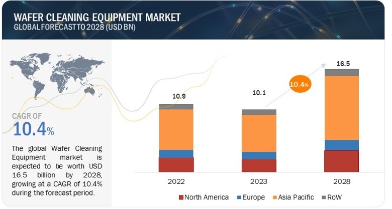
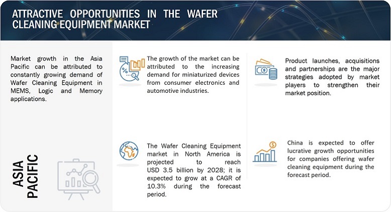
Wafer Cleaning Equipment Market

Wafer Cleaning Equipment Market

Wafer Cleaning Equipment Market Forecast to 2028

To know about the assumptions considered for the study, Request for Free Sample Report

Wafer Cleaning Equipment Market Dynamics

Driver: Growing demand for memory devices from AI-based servers

In recent years, there has been a significant surge in the adoption of artificial intelligence (AI) for various applications. The constantly growing generative AI market owing to the increasing popularity of AI-based chatbots such as ChatGPT is a major factor fueling the growth of the generative AI market. The growing popularity of such AI-based chatbots is expected to drive the demand for memory and storage devices, subsequently improving their average selling price (ASP) trends especially in the next 5 years. The improving price trend of memory and storage devices is also expected to help manufacturers of memory and storage devices to reduce excess inventory. The growing adoption of memory-based devices and subsequently increasing shipments of memory devices globally is expected to drive the growth of the semiconductor industry, thereby fueling the market growth for wafer cleaning equipment.

Restraint: Environmental concerns owing to emission of hazardous chemicals during wafer cleaning

Wafer cleaning is one of the most recurrent steps in the process manufacturing semiconductor devices. However, the growing trend of miniaturization and subsequently shrinking dimensions of devices have resulted in an increase in the levels of impurities. In the wafer fabrication and cleaning processes, some of the toxic chemicals and acids such as antimony (Sb), antimony trioxide (SbO3), arsenic pentafluoride (AsF5), arsenic (As), boron trichloride (BCl3), boron trifluoride (BF3), chlorine (Cl), germane (GeH4), hydrogen sulfide (H2S), hydrogen peroxide (H2O2), and oxidized carbon are used. All these chemicals are hazardous and toxic and have an adverse impact on human health and the environment. Hence, they must be used in a controlled environment. Furthermore, wet chemical cleaning process, a commonly used cleaning technology that helps in removing damage and contamination in the wafer uses substantial amounts of chemicals and acids which are harmful to the environment. However, technological advancements and the emergence of alternatives such as dry-cleaning processes such as plasma cleaning, short wavelength, and ultraviolet radiation is expected to reduce the adverse impact of wafer cleaning on the environment on a longer run.

Opportunity: Technological advancements

There have been several technological advancements related to compound semiconductor technologies in recent years. For instance, GaN semiconductor devices have witnessed several technological advancements that have driven their demand in various applications. Advancements in GaN crystal growth techniques such as metal organic chemical vapor deposition (MOCVD) and molecular epitaxy (MBE) are implemented in their manufacturing processes. These techniques deliver high-quality GaN materials with lower defect densities. Researchers are also exploring alternative substrates for GaN epitaxial layers such as GaN-on-Silicon technology as it reduces the cost of GaN devices and improves thermal performance, whereas GaN-on-GaN technology is emerging as it allows GaN semiconductor devices to have high breakdown tolerance and scalability. Constantly emerging technological advancements related to compound semiconductor devices is expected to create a surge in the production of discrete and integrated semiconductor devices such as transistors, diodes, amplifiers, ICs, etc., subsequently increasing the need for wafer cleaning.

Challenge: Longer construction timelines for new fabs in the US

The development of a new fab takes about 2 to 4 years in any country. However, the number of days taken in the US to develop a new fab is more than Japan, China, and Taiwan. The US has several environmental, health, and safety (EHS) regulations enforced by the federal governments that must be adhered to during the construction of a new semiconductor manufacturing facility. Though the regulations are instrumental in reducing the adverse environmental impact, they significantly reduce the pace of construction of new and advanced fabrication facilities in the US. Conventionally, the Clean Air Act (1970), and other hazardous waste regulations were the major regulations that were adhered to during the development of a new fabrication facility. However, the Council on Environmental Quality’s (CEQ’s) National Environmental Policy Act (NEPA) and the passage of CHIPS Act in 2022 had further increased in the time taken for the construction of new fabrication facilities in the US as these regulations are applicable to all the projects funded by the federal governments. Stringent government regulations in the US are expected to significantly increase the time taken for the construction of new fabrication facilities in the country.

Wafer Cleaning Equipment Market Ecosystem
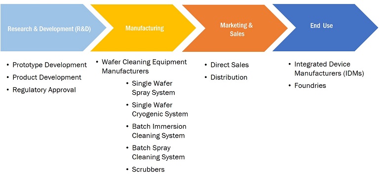
Wafer Cleaning Equipment Market by Ecosystem

The single wafer spray system is expected to grow at the highest CAGR of the wafer cleaning equipment market during the forecast period

In the wafer cleaning process, contamination and impurities can have a detrimental effect on the performance of devices. These contaminations and impurities need to be removed during semiconductor manufacturing to obtain high-quality devices. On each successive decade, the dimensions of devices are shrinking and making the devices more exposed to mechanical forces applied to them during cleaning, possibly leading to defect formation. A single wafer spray cleaning system is a very promising cleaning system to remove impurities with minimal damage. In this cleaning system, a single wafer is placed for processing in a stationary spray column where the wafer is exposed to the mist of chemicals, such as SC-1, SC-2, and de-ionized water. During this process, the wafer is spun and rinsed. After spinning, the wafer is dried in an atmosphere of nitrogen (N2). These systems are quite expensive but are promising toward effective cleaning and causing minimal damage to a wafer.

Memory application is holds the largest market share in the wafer cleaning equipment market in 2022

Diverse forms of memory, including dynamic random access memory (DRAM), synchronous dynamic random access memory (SDRAM), and flash memory (NAND or NOR), find application in computers, laptops, digital music players, gaming devices, and mobile Internet devices. The creation of memory chips involves an initial process of cleaning an entire wafer from its rear surface, followed by the incorporation of the chip onto the wafer. This wafer is subjected to cleaning procedures facilitated by wafer cleaning equipment. In the present context, NAND flash memory has gained widespread usage in mobile electronics. As memory dimensions continue to decrease to the nanoscale, the cleansing and removal of defects from silicon wafers have emerged as pivotal tasks for achieving enhanced quality and efficiency. Precision cleaning is imperative for memory due to its sensitivity; inadequate cleaning can compromise its proper functionality.

Asia Pacific is expected to grow at the highest market share during the forecast period

For the past four and a half decades, the Asia-Pacific (APAC) region has wielded significant influence within the semiconductor equipment sector, shaping its trajectory in remarkable ways. The evolution of California's Silicon Valley since the 1970s owes a considerable debt to the support extended by stakeholders in the APAC region.

In the upcoming forecast period, the APAC region is projected to maintain its prominent position in the wafer cleaning equipment market. This dominance can be attributed to several factors, including the availability of cost-effective labor in China, the strides taken in innovation and enhancement of fabrication facilities in Taiwan, and the continuous advancement of semiconductor equipment manufacturing capabilities in Japan. These factors collectively contribute to a range of cutting-edge advantages that bolster the prowess of the Asian semiconductor industry. In the APAC region, the wafer cleaning equipment market is primarily led by key players situated in Taiwan, South Korea, Japan, and China. Among these, South Korea and Taiwan are anticipated to emerge as global frontrunners within the wafer cleaning equipment market as of 2022.
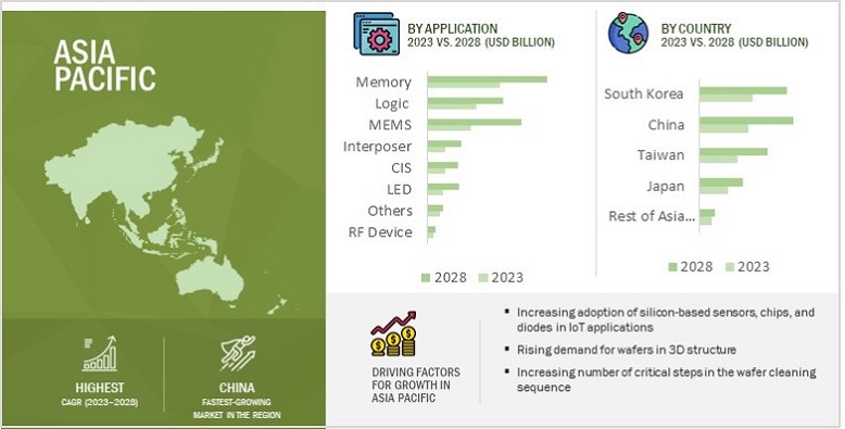
Wafer Cleaning Equipment Market by Region

Wafer Cleaning Equipment Market by Region

To know about the assumptions considered for the study, download the pdf brochure

Key Market Players

The major players in the wafer cleaning equipment companies include SCREEN Holdings Co., Ltd. (Japan), Tokyo Electron Limited (Japan), Applied Materials (US), LAM Research Corporation (US), Shibaura Mechatronics Corporation (Japan), PVA TePLA AG (Germany), Entregris Inc., (US), SEMES (US), Modutek.com (Japan), Veeco Instruments Inc. (US), Toho Technology (US), ULTRON SYSTEMS, INC. (US), Akrion Technologies (US), Axus Technology (US), SHIBAURA MECHATRONICS CORPORATION (Japan), etc. These companies have used both organic and inorganic growth strategies such as product launches, acquisitions, and partnerships to strengthen their position in the market.

Get online access to the report on the World's First Market Intelligence Cloud

  • Easy to Download Historical Data & Forecast Numbers
  • Company Analysis Dashboard for high growth potential opportunities
  • Research Analyst Access for customization & queries
  • Competitor Analysis with Interactive dashboard
  • Latest News, Updates & Trend analysis
Request Sample

Scope of the Report

Report Metric

Details

Estimated Value USD 10.1 billion in 2023
Projected Value 16.5 billion by 2028
Growth Rate 10.4%

Market size available for years

2019–2028

Base year considered

2022

Forecast period

2023–2028

Forecast units

Value (USD Million/Billion), Volume (Million Square Inches)

Segments covered

By Equipment Type, Wafer Size, Application and Region

Geographies covered

North America, Europe, Asia Pacific, and Rest of World

Companies covered

The major players in the wafer cleaning equipment market are SCREEN Holdings Co., Ltd. (Japan), Tokyo Electron Limited (Japan), Lam Research Corporation (US), Applied Materials Inc, Inc. (US), Shibaura Mechatronics Corporation (Japan), Akrion Technologies (US), Modutek.com (US), PVA TePLA AG (Germany), Entegris (US), ULTRON SYSTEMS, INC. (US), Veeco Instruments Inc. (US), SEMES (South Korea), AXUS Technology (US), Beijing TSD Semiconductor Equipment Co., Ltd. (China), Toho Kasei Co., Ltd. (Japan), Cleaning Technologies Group (US), SEMETEK (US), AP&S International GmbH (Germany), ITW (US), RENA Technologies GmbH (Germany), TDC Co., Ltd. (Japan), Orbray Co., Ltd. (Japan), DAINICHI SHOJI K.K (China), and Ultra t Equipment Company Inc. (US).

Wafer Cleaning Equipment Market Highlights

The study segments the wafer cleaning equipment market based on hardware, software, services, vertical, and region at the regional and global level.

Segment

Subsegment

By Equipment Type

  • Single Wafer Spray System
  • Single Wafer Cryogenic System
  • Batch Immersion Cleaning System
  • Batch Spray Cleaning System
  • Scrubbers

By Wafer Size

  • Less than Equals 150 mm
  • 200 mm
  • 300 mm

By Application

  • MEMS
  • CIS
  • Memory
  • Logic
  • RF Devices
  • LED
  • Interposer
  • Others

By Region

  • North America
  • Europe
  • Asia Pacific
  • Rest of the World

Recent Developments

  • In July 2023, Tokyo Electron Limited has announced the completion of its new development building at the Hosaka Office in Yamanashi Prefecture. This expansion enhances TEL's technology development capabilities, supporting the growth of products crucial for the semiconductor market's advancements.
  • In January 2023, SCREEN Holdings Co., Ltd. has completed the construction of its new factory (S-Cube 4), dedicated to semiconductor production equipment. The facility was built at the existing Hikone Site and marks a significant development for the company's semiconductor manufacturing capabilities.
  • In December 2022, SCREEN SPE introduces the SU-3400, a single wafer cleaning system with world-leading throughput and unique cleaning technologies. The system's innovative design with six-level stacked towers and downsized cleaning chambers reduces its footprint by 30%. Equipped with 24 chambers, the SU-3400 achieves a high practical processing capacity of up to 1,200 wafers per hour.
  • In December 2022, SCREEN Semiconductor Solutions Co., Ltd. and imec have renewed their joint development agreement to collaborate on developing advanced and sustainable technologies. This partnership leverages SCREEN's expertise in wafer cleaning technology and imec's prowess in nanoelectronics and digital technologies.
  • In November 2022, Lam Research Corporation acquired SEMSYSCO GmbH, a global provider of wet processing semiconductor equipment, from Gruenwald Equity and other investors. This acquisition has enriched Lam's capabilities in advanced packaging, particularly suitable for state-of-the-art logic chips and chiplet-based solutions catering to high-performance computing (HPC), artificial intelligence (AI), and other data-intensive applications.

Frequently Asked Questions (FAQs):

To speak to our analyst for a discussion on the above findings, click Speak to Analyst

TABLE OF CONTENTS
 
1 INTRODUCTION (Page No. - 31)
    1.1 STUDY OBJECTIVES 
    1.2 MARKET DEFINITION 
    1.3 STUDY SCOPE 
           1.3.1 INCLUSIONS AND EXCLUSIONS
           1.3.2 MARKETS COVERED
           1.3.3 REGIONAL SCOPE
           1.3.4 YEARS CONSIDERED
    1.4 CURRENCY CONSIDERED 
    1.5 PACKAGE SIZE 
    1.6 LIMITATIONS 
    1.7 STAKEHOLDERS 
    1.8 SUMMARY OF CHANGES 
    1.9 RECESSION IMPACT 
 
2 RESEARCH METHODOLOGY (Page No. - 36)
    2.1 RESEARCH DATA 
           FIGURE 1 WAFER CLEANING EQUIPMENT MARKET: RESEARCH DESIGN
           2.1.1 SECONDARY DATA
                    2.1.1.1 Key data from secondary sources
                    2.1.1.2 Key secondary sources
           2.1.2 PRIMARY DATA
                    2.1.2.1 Key data from primary sources
                    2.1.2.2 Primary research participants across supply side
                    2.1.2.3 Breakdown of primary interviews
                    2.1.2.4 Key industry insights
           2.1.3 SECONDARY AND PRIMARY RESEARCH
    2.2 MARKET SIZE ESTIMATION 
           FIGURE 2 MARKET SIZE ESTIMATION METHODOLOGY: APPROACH 1 (SUPPLY SIDE): REVENUE GENERATED BY KEY PLAYERS IN WAFER CLEANING EQUIPMENT MARKET
           FIGURE 3 MARKET SIZE ESTIMATION METHODOLOGY: APPROACH 2 (SUPPLY SIDE): ILLUSTRATION OF REVENUE ESTIMATION OF KEY PLAYERS IN WAFER CLEANING EQUIPMENT MARKET
           FIGURE 4 MARKET SIZE ESTIMATION METHODOLOGY: APPROACH 3 (DEMAND SIDE) –BOTTOM-UP APPROACH TO ESTIMATE WAFER CLEANING EQUIPMENT MARKET SIZE BASED ON REGION
           2.2.1 BOTTOM-UP APPROACH
                    2.2.1.1 Estimation of market size using bottom-up approach
                               FIGURE 5 MARKET SIZE ESTIMATION METHODOLOGY: BOTTOM-UP APPROACH
           2.2.2 TOP-DOWN APPROACH
                    2.2.2.1 Estimation of market size using top-down approach
                               FIGURE 6 MARKET SIZE ESTIMATION METHODOLOGY: TOP-DOWN APPROACH
    2.3 MARKET SHARE CALCULATION 
    2.4 DATA TRIANGULATION 
           FIGURE 7 DATA TRIANGULATION
    2.5 RISK ASSESSMENT 
           TABLE 1 RISK FACTOR ANALYSIS
           2.5.1 IMPACT OF RECESSION ON GDP
    2.6 RESEARCH ASSUMPTIONS AND LIMITATIONS 
           2.6.1 RESEARCH ASSUMPTIONS
           2.6.2 RESEARCH LIMITATIONS
 
3 EXECUTIVE SUMMARY (Page No. - 51)
    FIGURE 8 WAFER CLEANING EQUIPMENT MARKET, 2019–2028
    FIGURE 9 BATCH SPRAY CLEANING SYSTEMS TO ACCOUNT FOR LARGEST SHARE OF WAFER CLEANING EQUIPMENT MARKET, BY EQUIPMENT TYPE, IN 2028
    FIGURE 10 300 MM WAFERS TO DOMINATE WAFER MARKET DURING FORECAST PERIOD
    FIGURE 11 MEMORY DEVICES TO LEAD WAFER CLEANING EQUIPMENT MARKET, BY APPLICATION, DURING FORECAST PERIOD
    FIGURE 12 ASIA PACIFIC TO RECORD HIGHEST CAGR IN GLOBAL WAFER CLEANING EQUIPMENT MARKET FROM 2023 TO 2028
 
4 PREMIUM INSIGHTS (Page No. - 55)
    4.1 ATTRACTIVE OPPORTUNITIES FOR PLAYERS IN WAFER CLEANING EQUIPMENT MARKET 
           FIGURE 13 GROWING POPULARITY OF 3D ICS TO BOOST DEMAND FOR WAFER CLEANING EQUIPMENT IN COMING YEARS
    4.2 WAFER CLEANING EQUIPMENT MARKET, BY EQUIPMENT TYPE 
           FIGURE 14 BATCH SPRAY CLEANING SYSTEMS TO CAPTURE LARGEST SHARE OF WAFER CLEANING EQUIPMENT MARKET IN 2023
    4.3 WAFER MARKET, BY WAFER SIZE 
           FIGURE 15 300 MM WAFERS TO ACCOUNT FOR LARGEST MARKET SHARE IN 2023
    4.4 WAFER CLEANING EQUIPMENT MARKET, BY APPLICATION 
           FIGURE 16 MEMORY DEVICES TO CAPTURE LARGEST SHARE OF WAFER CLEANING EQUIPMENT MARKET IN 2023
    4.5 WAFER CLEANING EQUIPMENT MARKET IN ASIA PACIFIC, BY APPLICATION AND COUNTRY 
           FIGURE 17 MEMORY DEVICES AND CHINA HELD LARGEST SHARE OF WAFER CLEANING EQUIPMENT MARKET IN ASIA PACIFIC, BY APPLICATION AND COUNTRY, RESPECTIVELY, IN 2022
 
5 MARKET OVERVIEW (Page No. - 58)
    5.1 INTRODUCTION 
    5.2 MARKET DYNAMICS 
           FIGURE 18 MARKET DYNAMICS: WAFER CLEANING EQUIPMENT MARKET
           5.2.1 DRIVERS
                    5.2.1.1 Increasing adoption of MEMS technology across various industries
                    5.2.1.2 Growing demand for memory devices with exceptional speed and accuracy from AI-based servers
                    5.2.1.3 Increasing use of electric vehicles
                               FIGURE 19 ELECTRIC CAR SALES DATA, 2019–2023 (MILLION UNITS)
                    5.2.1.4 Surging adoption of 5G technology
                               FIGURE 20 5G MOBILE SUBSCRIPTIONS, 2019–2028 (MILLION UNITS)
                               FIGURE 21 IMPACT ANALYSIS OF DRIVERS ON WAFER CLEANING EQUIPMENT MARKET
           5.2.2 RESTRAINTS
                    5.2.2.1 Environmental concerns owing to emission of hazardous chemicals during wafer cleaning
                               FIGURE 22 IMPACT ANALYSIS OF RESTRAINTS ON WAFER CLEANING MARKET
           5.2.3 OPPORTUNITIES
                    5.2.3.1 Growing popularity of 3D ICs
                    5.2.3.2 Rising adoption of technologically advanced semiconductor devices
                    5.2.3.3 Increasing adoption of silicon-based semiconductor devices in IoT applications
                               FIGURE 23 IMPACT ANALYSIS OF OPPORTUNITIES ON WAFER CLEANING EQUIPMENT MARKET
           5.2.4 CHALLENGES
                    5.2.4.1 Possibility of water shortage in semiconductor fab facilities globally
                    5.2.4.2 Longer construction timelines associated with new semiconductor fabs in US due to stringent regulations
                               FIGURE 24 IMPACT ANALYSIS OF CHALLENGES ON WAFER CLEANING EQUIPMENT MARKET
    5.3 SUPPLY CHAIN ANALYSIS 
           FIGURE 25 WAFER CLEANING EQUIPMENT SUPPLY CHAIN ANALYSIS
           TABLE 2 PARTICIPANTS AND THEIR ROLE IN ECOSYSTEM
    5.4 ECOSYSTEM MAPPING 
           5.4.1 WAFER CLEANING EQUIPMENT ECOSYSTEM ANALYSIS
                     FIGURE 26 WAFER CLEANING EQUIPMENT ECOSYSTEM
           5.4.2 WAFER CLEANING STEPS (RCA CLEAN PROCESS)
                    5.4.2.1 First step (SC-1): Organic and particle cleaning
                    5.4.2.2 Second step: Oxide stripping
                    5.4.2.3 Third step (SC-2): Ionic cleaning
                    5.4.2.4 Rinsing and drying (optional process)
                               FIGURE 27 WAFER CLEANING OBJECTIVES
                               TABLE 3 SOLUTIONS/MIXTURES/COMPOUNDS USED IN WAFER CLEANING APPLICATIONS
    5.5 TECHNOLOGY TRENDS 
           5.5.1 PIRANHA ETCH CLEANING
           5.5.2 MEGASONIC CLEANING
           5.5.3 OZONE CLEANING
    5.6 INDICATIVE PRICE ANALYSIS 
           TABLE 4 INDICATIVE PRICE OF SINGLE-WAFER SPRAY SYSTEMS
           TABLE 5 INDICATIVE PRICE OF CHEMICALS USED IN WAFER CLEANING
    5.7 PATENT ANALYSIS 
           TABLE 6 PATENTS FILED AND GRANTED, JANUARY 2012–DECEMBER 2022
           FIGURE 28 NUMBER OF PATENTS GRANTED FOR WAFER CLEANING EQUIPMENT, 2012–2022
           FIGURE 29 TOP 10 COMPANIES WITH HIGHEST NUMBER OF PATENT APPLICATIONS, JANUARY 2012–DECEMBER 2022
           TABLE 7 TOP 20 PATENT OWNERS, JANUARY 2012–DECEMBER 2022
    5.8 PORTER’S FIVE FORCES ANALYSIS 
           FIGURE 30 WAFER CLEANING EQUIPMENT MARKET: PORTER’S FIVE FORCES ANALYSIS, 2022
           FIGURE 31 IMPACT ANALYSIS OF PORTER’S FIVE FORCES ON WAFER CLEANING EQUIPMENT MARKET, 2022
           TABLE 8 WAFER CLEANING EQUIPMENT MARKET: PORTER’S FIVE FORCES ANALYSIS, 2022
           5.8.1 THREAT OF NEW ENTRANTS
           5.8.2 THREAT OF SUBSTITUTES
           5.8.3 BARGAINING POWER OF SUPPLIERS
           5.8.4 BARGAINING POWER OF BUYERS
           5.8.5 INTENSITY OF COMPETITIVE RIVALRY
    5.9 KEY STAKEHOLDERS AND BUYING CRITERIA 
           5.9.1 KEY STAKEHOLDERS IN BUYING PROCESS
                    FIGURE 32 INFLUENCE OF STAKEHOLDERS ON BUYING PROCESS OF WAFER CLEANING EQUIPMENT, BY WAFER SIZE
                    TABLE 9 INFLUENCE OF STAKEHOLDERS ON BUYING PROCESS OF WAFER CLEANING EQUIPMENT, BY WAFER SIZE (%)
           5.9.2 BUYING CRITERIA
           FIGURE 33 KEY BUYING CRITERIA FOR WAFER CLEANING EQUIPMENT, BY WAFER SIZE
           TABLE 10 KEY BUYING CRITERIA FOR WAFER CLEANING EQUIPMENT, BY WAFER SIZE
    5.10 CASE STUDIES 
           5.10.1 ECO-SNOW SYSTEMS COLLABORATES WITH OWENS DESIGN TO DEVELOP 300 MM WAFER CLEANING PLATFORM TO REMOVE IMPURITIES
           5.10.2 LEADING PROVIDER OF WAFER CLEANING EQUIPMENT COLLABORATES WITH TISMO TECHNOLOGY SOLUTIONS TO DEVELOP HMI SYSTEM FOR PLASMA CLEANING
    5.11 TRADE DATA ANALYSIS 
           TABLE 11 EXPORT DATA FOR SEMICONDUCTOR MANUFACTURING MACHINES IN MAJOR COUNTRIES, 2018–2022 (USD MILLION)
           FIGURE 34 EXPORT VALUES FOR SEMICONDUCTOR MANUFACTURING MACHINES IN MAJOR COUNTRIES, 2018–2022
           TABLE 12 IMPORT DATA FOR SEMICONDUCTOR MANUFACTURING MACHINES IN MAJOR COUNTRIES, 2018–2022 (USD MILLION)
           FIGURE 35 IMPORT VALUES FOR SEMICONDUCTOR MANUFACTURING MACHINES IN MAJOR COUNTRIES, 2018–2022
    5.12 TARIFF AND REGULATORY LANDSCAPE 
           5.12.1 TARIFFS
                    TABLE 13 MFN TARIFFS FOR SEMICONDUCTOR MANUFACTURING EQUIPMENT EXPORTED BY US
           5.12.2 REGULATORY BODIES, GOVERNMENT AGENCIES, AND OTHER ORGANIZATIONS
                    5.12.2.1 North America
                    5.12.2.2 Europe
                    5.12.2.3 Asia Pacific
                    5.12.2.4 RoW
           5.12.3 REGULATIONS
           5.12.4 STANDARDS
    5.13 TRENDS/DISRUPTIONS IMPACTING CUSTOMER BUSINESS 
           FIGURE 36 REVENUE SHIFT AND NEW REVENUE POCKETS FOR WAFER CLEANING EQUIPMENT MARKET
    5.14 KEY CONFERENCES AND EVENTS, 2023–2024 
           TABLE 14 WAFER CLEANING EQUIPMENT MARKET: LIST OF CONFERENCES AND EVENTS
 
6 OPERATING MODES OF WAFER CLEANING EQUIPMENT (Page No. - 86)
    6.1 INTRODUCTION 
    6.2 AUTOMATIC 
    6.3 SEMIAUTOMATIC 
    6.4 MANUAL 
 
7 TECHNOLOGIES AND PROCESSES USED IN WAFER CLEANING (Page No. - 87)
    7.1 INTRODUCTION 
    7.2 WET CHEMICAL CLEANING 
           FIGURE 37 WET CHEMICAL CLEANING PROCESS
           7.2.1 USE OF HF ACID SOLUTION IN WET CLEANING PROCESS
           7.2.2 USE OF SULFURIC ACID IN WET CLEANING PROCESS
           7.2.3 RCA CLEANING PROCESS
           7.2.4 ALTERNATIVE CLEANING PROCESSES
    7.3 VAPOR DRY CLEANING 
           7.3.1 VAPOR PHASE CLEANING
           7.3.2 PLASMA STRIPPING CLEANING
    7.4 AQUEOUS CLEANING 
           FIGURE 38 STANDARD WAFER CLEANING PROCESS
           7.4.1 AQUEOUS FEOL CLEANING
           7.4.2 AQUEOUS BEOL CLEANING
    7.5 CRYOGENIC AEROSOLS AND SUPER-CRITICAL FLUID CLEANING 
    7.6 EMERGING TECHNOLOGIES 
           7.6.1 LASER CLEANING TECHNOLOGIES
                    7.6.1.1 Dry laser cleaning
                    7.6.1.2 Steam laser cleaning
           7.6.2 AQUEOUS-BASED EMERGING TECHNOLOGIES
                    7.6.2.1 Foam/bubble cleaning
                    7.6.2.2 Immersion pressure pulsation cleaning
                    7.6.2.3 Spray pressure pulsation cleaning
           7.6.3 CHEMICAL-BASED EMERGING TECHNOLOGIES
           7.6.4 DRY PARTICLE REMOVING TECHNOLOGIES
                    7.6.4.1 Liquid clusters
                    7.6.4.2 Nonoprobe cleaning
 
8 ANALYSIS OF IMPURITIES IN WAFER CLEANING PROCESSES AND EQUIPMENT (Page No. - 93)
    8.1 INTRODUCTION 
           TABLE 15 IMPACT OF IMPURITIES ON WAFERS, BY CONTAMINANT TYPE
    8.2 METALS 
    8.3 PARTICULATES 
    8.4 CHEMICALS 
 
9 WAFER MARKET, BY WAFER SIZE (Page No. - 96)
    9.1 INTRODUCTION 
           FIGURE 39 300 MM WAFERS TO REGISTER HIGHEST CAGR DURING FORECAST PERIOD
           TABLE 16 WAFER MARKET, BY WAFER SIZE, 2019–2022 (MILLION SQUARE INCHES)
           TABLE 17 WAFER MARKET, BY WAFER SIZE, 2023–2028 (MILLION SQUARE INCHES)
    9.2 ≤150 MM 
           9.2.1 EMERGENCE OF WAFERS WITH LARGER DIAMETERS TO ADVERSELY IMPACT ADOPTION OF SMALLER DIAMETER WAFERS
                    TABLE 18 ≤150 MM: WAFER MARKET, BY APPLICATION, 2019–2022 (MILLION SQUARE INCHES)
                    TABLE 19 ≤150 MM: WAFER MARKET, BY APPLICATION, 2023–2028 (MILLION SQUARE INCHES)
    9.3 200 MM 
           9.3.1 RISING ADOPTION OF 200 MM WAFERS TO BALANCE PRODUCTION EFFICIENCY AND YIELD RATES TO DRIVE MARKET
                    TABLE 20 200 MM: WAFER MARKET, BY APPLICATION, 2019–2022 (MILLION SQUARE INCHES)
                    TABLE 21 200 MM: WAFER MARKET, BY APPLICATION, 2023–2028 (MILLION SQUARE INCHES)
 
    9.4 300 MM 
           9.4.1 ABILITY OF 300 MM WAFERS TO FACILITATE ADVANCED FABRICATION TECHNIQUES TO DRIVE ADOPTION IN MEMORY CHIPS AND ICS
                    FIGURE 40 MEMORY DEVICES TO HOLD LARGEST SHARE OF 300 MM WAFER MARKET IN 2028
                    TABLE 22 300 MM: WAFER MARKET, BY APPLICATION, 2019–2022 (MILLION SQUARE INCHES)
                    TABLE 23 300 MM: WAFER MARKET, BY APPLICATION, 2023–2028 (MILLION SQUARE INCHES)
 
10 WAFER CLEANING EQUIPMENT MARKET, BY EQUIPMENT TYPE (Page No. - 103)
     10.1 INTRODUCTION 
             TABLE 24 WAFER CLEANING EQUIPMENT MARKET, BY EQUIPMENT TYPE, 2019–2022 (USD MILLION)
             FIGURE 41 BATCH SPRAY CLEANING SYSTEMS TO HOLD LARGEST SHARE OF WAFER CLEANING EQUIPMENT MARKET IN 2028
             TABLE 25 WAFER CLEANING EQUIPMENT MARKET, BY EQUIPMENT TYPE, 2023–2028 (USD MILLION)
     10.2 SINGLE-WAFER CLEANING SYSTEMS 
             10.2.1 ABILITY OF SINGLE-WAFER CLEANING SYSTEMS TO EFFICIENTLY CLEAN WAFER WITH MINIMAL DAMAGE TO DRIVE MARKET
                        TABLE 26 SINGLE-WAFER SPRAY SYSTEMS: WAFER CLEANING EQUIPMENT MARKET, BY APPLICATION, 2019–2022 (USD MILLION)
                        FIGURE 42 MEMORY DEVICES TO CAPTURE LARGEST SHARE OF SINGLE-WAFER SPRAY SYSTEM MARKET THROUGHOUT FORECAST PERIOD
                        TABLE 27 SINGLE-WAFER SPRAY SYSTEMS: WAFER CLEANING EQUIPMENT MARKET, BY APPLICATION, 2023–2028 (USD MILLION)
     10.3 SINGLE-WAFER CRYOGENIC SYSTEMS 
             10.3.1 POTENTIAL TO REMOVE CONTAMINANTS AT ULTRA-LOW TEMPERATURE TO BOOST ADOPTION OF SINGLE-WAFER CRYOGENIC SYSTEMS
                        TABLE 28 SINGLE-WAFER CRYOGENIC SYSTEMS: WAFER CLEANING EQUIPMENT MARKET, BY APPLICATION, 2019–2022 (USD MILLION)
                        FIGURE 43 MEMORY DEVICES TO DOMINATE SINGLE-WAFER CRYOGENIC SYSTEM MARKET IN 2028
                        TABLE 29 SINGLE-WAFER CRYOGENIC SYSTEMS: WAFER CLEANING EQUIPMENT MARKET, BY APPLICATION, 2023–2028 (USD MILLION)
     10.4 BATCH IMMERSION CLEANING SYSTEMS 
             10.4.1 PROFICIENCY IN CLEANING MULTIPLE WAFERS SIMULTANEOUSLY TO FUEL DEPLOYMENT OF BATCH IMMERSION CLEANING SYSTEMS
                        TABLE 30 BATCH IMMERSION CLEANING SYSTEMS: WAFER CLEANING EQUIPMENT MARKET, BY APPLICATION, 2019–2022 (USD MILLION)
                        FIGURE 44 MEMS DEVICES TO EXHIBIT HIGHEST CAGR IN BATCH IMMERSION SYSTEM MARKET DURING FORECAST PERIOD
                        TABLE 31 BATCH IMMERSION CLEANING SYSTEMS: WAFER CLEANING EQUIPMENT MARKET, BY APPLICATION, 2023–2028 (USD MILLION)
     10.5 BATCH SPRAY CLEANING SYSTEMS 
             10.5.1 COMPETENCY IN HANDLING LARGE BATCHES WITH HIGH THROUGHPUT TO INCREASE IMPLEMENTATION OF BATCH SPRAY CLEANING SYSTEMS
                        TABLE 32 BATCH SPRAY CLEANING SYSTEMS: WAFER CLEANING EQUIPMENT MARKET, BY APPLICATION, 2019–2022 (USD MILLION)
                        FIGURE 45 LEDS TO EXHIBIT SECOND-HIGHEST CAGR IN BATCH SPRAY CLEANING SYSTEM MARKET DURING FORECAST PERIOD
                        TABLE 33 BATCH SPRAY CLEANING SYSTEMS: WAFER CLEANING EQUIPMENT MARKET, BY APPLICATION, 2023–2028 (USD MILLION)
     10.6 SCRUBBERS 
             10.6.1 CAPABILITY TO REMOVE TINY PARTICLES ON WAFERS TO DRIVE DEMAND FOR SCRUBBERS
                        TABLE 34 SCRUBBERS: WAFER CLEANING EQUIPMENT MARKET, BY APPLICATION, 2019–2022 (USD MILLION)
                        FIGURE 46 MEMS DEVICES TO RECORD HIGHEST CAGAR IN SCRUBBER MARKET DURING FORECAST PERIOD
                        TABLE 35 SCRUBBERS: WAFER CLEANING EQUIPMENT MARKET, BY APPLICATION, 2023–2028 (USD MILLION)
 
11 WAFER CLEANING EQUIPMENT MARKET, BY APPLICATION (Page No. - 116)
     11.1 INTRODUCTION 
             TABLE 36 WAFER CLEANING EQUIPMENT MARKET, BY APPLICATION, 2019–2022 (USD MILLION)
             FIGURE 47 MEMORY DEVICES TO DOMINATE WAFER CLEANING EQUIPMENT MARKET THROUGHOUT FORECAST PERIOD
             TABLE 37 WAFER CLEANING EQUIPMENT MARKET, BY APPLICATION, 2023–2028 (USD MILLION)
             TABLE 38 WAFER MARKET, BY APPLICATION, 2019–2022 (MILLION SQUARE INCH)
             TABLE 39 WAFER MARKET, BY APPLICATION, 2023–2028 (MILLION SQUARE INCH)
     11.2 COMPETITOR ANALYSIS 
     11.3 MEMS DEVICES 
             11.3.1 HIGH DEMAND FOR MEMS DEVICES FROM CONSUMER ELECTRONICS MANUFACTURERS TO DRIVE MARKET
                        TABLE 40 MEMS DEVICES: WAFER CLEANING EQUIPMENT MARKET, BY REGION, 2019–2022 (USD MILLION)
                        TABLE 41 MEMS DEVICES: WAFER CLEANING EQUIPMENT MARKET, BY REGION, 2023–2028 (USD MILLION)
                        TABLE 42 MEMS DEVICES: WAFER CLEANING EQUIPMENT MARKET IN ASIA PACIFIC, BY COUNTRY, 2019–2022 (USD MILLION)
                        TABLE 43 MEMS DEVICES: WAFER CLEANING EQUIPMENT MARKET IN ASIA PACIFIC, BY COUNTRY, 2023–2028 (USD MILLION)
                        TABLE 44 MEMS DEVICES: WAFER CLEANING EQUIPMENT MARKET, BY EQUIPMENT TYPE, 2019–2022 (USD MILLION)
                        FIGURE 48 SINGLE-WAFER SPRAY SYSTEMS TO LEAD WAFER CLEANING EQUIPMENT MARKET FOR MEMS APPLICATIONS DURING FORECAST PERIOD
                        TABLE 45 MEMS DEVICES: WAFER CLEANING EQUIPMENT MARKET, BY EQUIPMENT TYPE, 2023–2028 (USD MILLION)
                        TABLE 46 MEMS DEVICES: WAFER MARKET, BY WAFER SIZE, 2019–2022 (MILLION SQUARE INCHES)
                        TABLE 47 MEMS DEVICES: WAFER MARKET, BY WAFER SIZE, 2023–2028 (MILLION SQUARE INCHES)
     11.4 CIS 
             11.4.1 RISING ADOPTION OF CMOS IMAGE SENSORS IN AEROSPACE AND MEDICAL IMAGING APPLICATIONS TO BOOST DEMAND FOR WAFER CLEANING EQUIPMENT
                        TABLE 48 CIS: WAFER CLEANING EQUIPMENT, BY REGION, 2019–2022 (USD MILLION)
                        TABLE 49 CIS: WAFER CLEANING EQUIPMENT, BY REGION, 2023–2028 (USD MILLION)
                        TABLE 50 CIS: WAFER CLEANING EQUIPMENT MARKET IN ASIA PACIFIC, BY COUNTRY, 2019–2022 (USD MILLION)
                        TABLE 51 CIS: WAFER CLEANING EQUIPMENT MARKET IN ASIA PACIFIC, BY COUNTRY, 2023–2028 (USD MILLION)
                        TABLE 52 CIS: WAFER CLEANING EQUIPMENT MARKET EQUIPMENT TYPE, 2019–2022 (USD MILLION)
                        FIGURE 49 BATCH SPRAY CLEANING SYSTEMS TO ACCOUNT FOR LARGEST SHARE OF WAFER CLEANING EQUIPMENT MARKET FOR CIS APPLICATIONS IN 2030
                        TABLE 53 CIS: WAFER CLEANING EQUIPMENT MARKET, BY EQUIPMENT TYPE, 2023–2028 (USD MILLION)
                        TABLE 54 CIS: WAFER MARKET, BY WAFER SIZE, 2019–2022 (MILLION SQUARE INCHES)
                        TABLE 55 CIS: WAFER MARKET, BY WAFER SIZE, 2023–2028 (MILLION SQUARE INCHES)
     11.5 MEMORY DEVICES 
             11.5.1 INCREASING DEPLOYMENT OF NAND FLASH MEMORY CHIPS IN CONSUMER ELECTRONICS TO SUPPORT MARKET GROWTH
                        TABLE 56 MEMORY DEVICES: WAFER CLEANING EQUIPMENT MARKET, BY REGION, 2019–2022 (USD MILLION)
                        TABLE 57 MEMORY DEVICES: WAFER CLEANING EQUIPMENT MARKET, BY REGION, 2023–2028 (USD MILLION)
                        TABLE 58 MEMORY DEVICES: WAFER CLEANING EQUIPMENT MARKET IN ASIA PACIFIC, BY COUNTRY, 2019–2022 (USD MILLION)
                        TABLE 59 MEMORY DEVICES: WAFER CLEANING EQUIPMENT MARKET IN ASIA PACIFIC, BY COUNTRY, 2023–2028 (USD MILLION)
                        TABLE 60 MEMORY DEVICES: WAFER CLEANING EQUIPMENT MARKET, BY EQUIPMENT TYPE, 2019–2022 (USD MILLION)
                        FIGURE 50 SINGLE-WAFER SPRAY SYSTEMS TO COMMAND WAFER CLEANING EQUIPMENT MARKET FOR MEMORY DEVICES FROM 2023 TO 2028
                        TABLE 61 MEMORY DEVICES: WAFER CLEANING EQUIPMENT MARKET, BY EQUIPMENT TYPE, 2023–2028 (USD MILLION)
                        TABLE 62 MEMORY DEVICES: WAFER MARKET, BY WAFER SIZE, 2019–2022 (MILLION SQUARE INCHES)
                        TABLE 63 MEMORY DEVICES: WAFER, BY WAFER SIZE, 2023–2028 (MILLION SQUARE INCHES)
     11.6 RF DEVICES 
             11.6.1 RISING INTEGRATION OF RF DEVICES INTO SMARTPHONES TO CONTRIBUTE TO MARKET GROWTH
                        TABLE 64 RF DEVICES: WAFER CLEANING EQUIPMENT MARKET, BY REGION, 2019–2022 (USD MILLION)
                        TABLE 65 RF DEVICES: WAFER CLEANING EQUIPMENT MARKET, BY REGION, 2023–2028 (USD MILLION)
                        TABLE 66 RF DEVICES: WAFER CLEANING EQUIPMENT MARKET IN ASIA PACIFIC, BY COUNTRY, 2019–2022 (USD MILLION)
                        TABLE 67 RF DEVICES: WAFER CLEANING EQUIPMENT MARKET IN ASIA PACIFIC, BY COUNTRY, 2023–2028 (USD MILLION)
                        TABLE 68 RF DEVICES: WAFER CLEANING EQUIPMENT MARKET, BY EQUIPMENT TYPE, 2019–2022 (USD MILLION)
                        FIGURE 51 BATCH IMMERSION CLEANING SYSTEMS TO HOLD LARGEST SHARE OF WAFER CLEANING EQUIPMENT MARKET FOR RF DEVICES IN 2028
                        TABLE 69 RF DEVICES: WAFER CLEANING EQUIPMENT MARKET, BY EQUIPMENT TYPE, 2023–2028 (USD MILLION)
                        TABLE 70 RF DEVICES: WAFER MARKET, BY WAFER SIZE, 2019–2022 (MILLION SQUARE INCHES)
                        TABLE 71 RF DEVICES: WAFER MARKET, BY WAFER SIZE, 2023–2028 (MILLION SQUARE INCHES)
     11.7 LEDS 
             11.7.1 INCREASING USE OF LEDS IN SMART LIGHTING SYSTEMS TO BOOST DEMAND FOR WAFER CLEANING EQUIPMENT
                        TABLE 72 LEDS: WAFER CLEANING EQUIPMENT MARKET, BY REGION, 2019–2022 (USD MILLION)
                        TABLE 73 LEDS: WAFER CLEANING EQUIPMENT MARKET, BY REGION, 2023–2028 (USD MILLION)
                        TABLE 74 LEDS: WAFER CLEANING EQUIPMENT MARKET IN ASIA PACIFIC, BY COUNTRY, 2019–2022 (USD MILLION)
                        TABLE 75 LEDS: WAFER CLEANING EQUIPMENT MARKET IN ASIA PACIFIC, BY COUNTRY, 2023–2028 (USD MILLION)
                        TABLE 76 LEDS: WAFER CLEANING EQUIPMENT MARKET, BY EQUIPMENT TYPE, 2019–2022 (USD MILLION)
                        FIGURE 52 BATCH SPRAY CLEANING SYSTEMS TO CAPTURE MAJORITY OF WAFER CLEANING EQUIPMENT MARKET SHARE FOR LEDS IN 2028
                        TABLE 77 LEDS: WAFER CLEANING EQUIPMENT MARKET, BY EQUIPMENT TYPE, 2023–2028 (USD MILLION)
                        TABLE 78 LEDS: WAFER MARKET, BY WAFER SIZE, 2019–2022 (MILLION SQUARE INCHES)
                        TABLE 79 LEDS: WAFER MARKET, BY WAFER SIZE, 2023–2028 (MILLION SQUARE INCHES)
     11.8 INTERPOSERS 
             11.8.1 SURGING DEMAND FOR ADVANCED PACKAGING SOLUTIONS TO DRIVE SEGMENTAL GROWTH
                        TABLE 80 INTERPOSERS: WAFER CLEANING EQUIPMENT MARKET, BY REGION, 2019–2022 (USD MILLION)
                        TABLE 81 INTERPOSERS: WAFER CLEANING EQUIPMENT MARKET, BY REGION, 2023–2028 (USD MILLION)
                        TABLE 82 INTERPOSERS: WAFER CLEANING EQUIPMENT MARKET IN ASIA PACIFIC, BY COUNTRY, 2019–2022 (USD MILLION)
                        TABLE 83 INTERPOSERS: WAFER CLEANING EQUIPMENT MARKET IN ASIA PACIFIC, BY COUNTRY, 2023–2028 (USD MILLION)
                        TABLE 84 INTERPOSERS: WAFER CLEANING EQUIPMENT MARKET, BY EQUIPMENT TYPE, 2019–2022 (USD MILLION)
                        FIGURE 53 BATCH SPRAY CLEANING SYSTEMS TO ACCOUNT FOR LARGEST MARKET SHARE FOR INTERPOSERS IN 2028
                        TABLE 85 INTERPOSERS: WAFER CLEANING EQUIPMENT MARKET, BY EQUIPMENT TYPE, 2023–2028 (USD MILLION)
                        TABLE 86 INTERPOSERS: WAFER MARKET, BY WAFER SIZE, 2019–2022 (MILLION SQUARE INCHES)
                        TABLE 87 INTERPOSERS: WAFER MARKET, BY WAFER SIZE, 2023–2028 (MILLION SQUARE INCHES)
     11.9 LOGIC DEVICES 
             11.9.1 GROWING DEPLOYMENT OF LOGIC DEVICES IN MICROPROCESSORS, MICROCONTROLLERS, AND GRAPHIC CHIPS TO ACCELERATE MARKET GROWTH
                        TABLE 88 LOGIC DEVICES: WAFER CLEANING EQUIPMENT MARKET, BY REGION, 2019–2022 (USD MILLION)
                        TABLE 89 LOGIC DEVICES: WAFER CLEANING EQUIPMENT MARKET, BY REGION, 2023–2028 (USD MILLION)
                        TABLE 90 LOGIC DEVICES: WAFER CLEANING EQUIPMENT MARKET IN ASIA PACIFIC, BY COUNTRY, 2019–2022 (USD MILLION)
                        TABLE 91 LOGIC DEVICES: WAFER CLEANING EQUIPMENT MARKET IN ASIA PACIFIC, BY COUNTRY, 2023–2028 (USD MILLION)
                        TABLE 92 LOGIC DEVICES: WAFER CLEANING EQUIPMENT MARKET, BY EQUIPMENT TYPE, 2019–2022 (USD MILLION)
                        FIGURE 54 BATCH SPRAY CLEANING SYSTEMS TO CAPTURE LARGEST SHARE OF WAFER CLEANING EQUIPMENT MARKET FOR LOGIC DEVICES IN 2028
                        TABLE 93 LOGIC DEVICES: WAFER CLEANING EQUIPMENT MARKET, BY EQUIPMENT TYPE, 2023–2028 (USD MILLION)
                        TABLE 94 LOGIC DEVICES: WAFER MARKET, BY WAFER SIZE, 2019–2022 (MILLION SQUARE INCHES)
                        TABLE 95 LOGIC DEVICES: WAFER MARKET, BY WAFER SIZE, 2023–2028 (MILLION SQUARE INCHES)
     11.1 OTHERS 
             TABLE 96 OTHERS: WAFER CLEANING EQUIPMENT MARKET, BY REGION, 2019–2022 (USD MILLION)
             TABLE 97 OTHERS: WAFER CLEANING EQUIPMENT MARKET, BY REGION, 2023–2028 (USD MILLION)
             TABLE 98 OTHERS: WAFER CLEANING EQUIPMENT MARKET IN ASIA PACIFIC, BY COUNTRY, 2019–2022 (USD MILLION)
             TABLE 99 OTHERS: WAFER CLEANING EQUIPMENT MARKET IN ASIA PACIFIC, BY COUNTRY, 2023–2028 (USD MILLION)
             TABLE 100 OTHERS: WAFER CLEANING EQUIPMENT MARKET, BY EQUIPMENT TYPE, 2019–2022 (USD MILLION)
             FIGURE 55 BATCH SPRAY CLEANING SYSTEMS TO DOMINATE WAFER CLEANING EQUIPMENT MARKET FOR OTHER APPLICATIONS FROM 2023 TO 2028
             TABLE 101 OTHERS: WAFER CLEANING EQUIPMENT MARKET, BY EQUIPMENT TYPE, 2023–2028 (USD MILLION)
             TABLE 102 OTHERS: WAFER MARKET, BY WAFER SIZE, 2019–2022 (MILLION SQUARE INCHES)
             TABLE 103 OTHERS: WAFER MARKET, BY WAFER SIZE, 2023–2028 (MILLION SQUARE INCHES)
 
12 WAFER CLEANING EQUIPMENT MARKET, BY REGION (Page No. - 147)
     12.1 INTRODUCTION 
             FIGURE 56 CHINA TO EXHIBIT HIGHEST CAGR IN GLOBAL WAFER CLEANING EQUIPMENT MARKET FROM 2023 TO 2028
             TABLE 104 WAFER CLEANING EQUIPMENT MARKET, BY REGION, 2019–2022 (USD MILLION)
             TABLE 105 WAFER CLEANING EQUIPMENT MARKET, BY REGION, 2023–2028 (USD MILLION)
     12.2 NORTH AMERICA 
             FIGURE 57 NORTH AMERICA: REGION SNAPSHOT
             TABLE 106 NORTH AMERICA: WAFER CLEANING EQUIPMENT MARKET, BY APPLICATION, 2019–2022 (USD MILLION)
             TABLE 107 NORTH AMERICA: WAFER CLEANING EQUIPMENT MARKET, BY APPLICATION, 2023–2028 (USD MILLION)
             TABLE 108 NORTH AMERICA: WAFER CLEANING EQUIPMENT MARKET, BY COUNTRY, 2019–2022 (USD MILLION)
             TABLE 109 NORTH AMERICA: WAFER CLEANING EQUIPMENT MARKET, BY COUNTRY, 2023–2028 (USD MILLION)
             12.2.1 NORTH AMERICA: RECESSION IMPACT
             12.2.2 US
                        12.2.2.1 Presence of manufacturing giants such as Intel and Global Foundries to drive market growth
             12.2.3 CANADA
                        12.2.3.1 Government-led initiatives promoting use of electric vehicles to support market growth
             12.2.4 MEXICO
                        12.2.4.1 Thriving telecommunications and energy sectors to fuel market growth
     12.3 EUROPE 
             FIGURE 58 EUROPE: REGION SNAPSHOT
             TABLE 110 EUROPE: WAFER CLEANING EQUIPMENT MARKET, BY APPLICATION, 2019–2022 (USD MILLION)
             TABLE 111 EUROPE: WAFER CLEANING EQUIPMENT MARKET, BY APPLICATION, 2023–2028 (USD MILLION)
             TABLE 112 EUROPE: WAFER CLEANING EQUIPMENT MARKET, BY COUNTRY, 2019–2022 (USD MILLION)
             TABLE 113 EUROPE: WAFER CLEANING EQUIPMENT MARKET, BY COUNTRY, 2023–2028 (USD MILLION)
             12.3.1 EUROPE: RECESSION IMPACT
             12.3.2 GERMANY
                        12.3.2.1 Presence of silicon foundries and chipmakers to drive market
             12.3.3 FRANCE
                        12.3.3.1 Growing focus on development of advanced communication network technologies to foster market growth
             12.3.4 ITALY
                        12.3.4.1 Existence of fabrication plants and OSAT companies to support market growth
             12.3.5 UK
                        12.3.5.1 Rising demand for electronic systems to contribute to market growth
             12.3.6 REST OF EUROPE
     12.4 ASIA PACIFIC 
             FIGURE 59 ASIA PACIFIC: REGION SNAPSHOT
             TABLE 114 ASIA PACIFIC: WAFER CLEANING EQUIPMENT MARKET, BY APPLICATION, 2019–2022 (USD MILLION)
             TABLE 115 ASIA PACIFIC: WAFER CLEANING EQUIPMENT MARKET, BY APPLICATION, 2023–2028 (USD MILLION)
             TABLE 116 ASIA PACIFIC: WAFER CLEANING EQUIPMENT MARKET, BY COUNTRY, 2019–2022 (USD MILLION)
             TABLE 117 ASIA PACIFIC: WAFER CLEANING EQUIPMENT MARKET, BY COUNTRY, 2023–2028 (USD MILLION)
             12.4.1 ASIA PACIFIC: RECESSION IMPACT
             12.4.2 TAIWAN
                        12.4.2.1 Presence of several giant OSAT vendors to fuel market growth
             12.4.3 CHINA
                        12.4.3.1 Strong focus on achieving self-reliance in memory and chip technologies to accelerate market growth
             12.4.4 JAPAN
                        12.4.4.1 Presence of prominent wafer cleaning equipment manufacturers to fuel market growth
             12.4.5 SOUTH KOREA
                        12.4.5.1 Government strategies to expedite growth of semiconductor industry to support market growth
             12.4.6 REST OF ASIA PACIFIC
     12.5 REST OF THE WORLD (ROW) 
             TABLE 118 ROW: WAFER CLEANING EQUIPMENT MARKET, BY APPLICATION, 2019–2022 (USD MILLION)
             TABLE 119 ROW: WAFER CLEANING EQUIPMENT MARKET, BY APPLICATION, 2023–2028 (USD MILLION)
             TABLE 120 ROW: WAFER CLEANING EQUIPMENT MARKET, BY REGION, 2019–2022 (USD MILLION)
             TABLE 121 ROW: WAFER CLEANING EQUIPMENT MARKET, BY REGION, 2023–2028 (USD MILLION)
             12.5.1 ROW: RECESSION IMPACT
             12.5.2 SOUTH AMERICA
                        12.5.2.1 Increasing demand for consumer electronics to drive market
             12.5.3 MIDDLE EAST & AFRICA
                        12.5.3.1 Rising use of connected devices and booming automotive industry to contribute to market growth
 
13 COMPETITIVE LANDSCAPE (Page No. - 166)
     13.1 OVERVIEW 
     13.2 MARKET EVALUATION FRAMEWORK 
             FIGURE 60 KEY STRATEGIES UNDERTAKEN BY LEADING PLAYERS IN WAFER CLEANING EQUIPMENT MARKET FROM 2021 TO 2023
     13.3 MARKET SHARE AND RANKING ANALYSIS 
             TABLE 122 WAFER CLEANING EQUIPMENT MARKET SHARE ANALYSIS, 2022
             FIGURE 61 MARKET SHARE OF TOP 5 PLAYERS PROVIDING WAFER CLEANING EQUIPMENT
     13.4 FIVE-YEAR COMPANY REVENUE ANALYSIS 
             FIGURE 62 FIVE-YEAR REVENUE ANALYSIS OF KEY COMPANIES
     13.5 COMPANY EVALUATION MATRIX, 2022 
             FIGURE 63 WAFER CLEANING EQUIPMENT MARKET (GLOBAL): COMPANY EVALUATION MATRIX, 2022
             13.5.1 STARS
             13.5.2 EMERGING LEADERS
             13.5.3 PERVASIVE PLAYERS
             13.5.4 PARTICIPANTS
     13.6 WAFER CLEANING EQUIPMENT MARKET: COMPANY FOOTPRINT 
             TABLE 123 OVERALL COMPANY FOOTPRINT (10 COMPANIES)
             TABLE 124 APPLICATION FOOTPRINT (10 COMPANIES)
             TABLE 125 REGION FOOTPRINT (10 COMPANIES)
     13.7 STARTUPS/SMES EVALUATION MATRIX, 2022 
             FIGURE 64 WAFER CLEANING EQUIPMENT (GLOBAL): STARTUPS/SMES EVALUATION MATRIX, 2022
             13.7.1 PROGRESSIVE COMPANIES
             13.7.2 RESPONSIVE COMPANIES
             13.7.3 DYNAMIC COMPANIES
             13.7.4 STARTING BLOCKS
     13.8 COMPETITIVE BENCHMARKING 
             TABLE 126 WAFER CLEANING EQUIPMENT MARKET: LIST OF KEY STARTUPS/SMES
             TABLE 127 WAFER CLEANING EQUIPMENT MARKET: COMPETITIVE BENCHMARKING OF KEY STARTUPS/SMES
     13.9 COMPETITIVE SCENARIO 
             13.9.1 PRODUCT LAUNCHES
                        TABLE 128 PRODUCT LAUNCHES, DECEMBER 2022–JANUARY 2023
             13.9.2 DEALS
                        TABLE 129 DEALS, JULY 2022–JULY 2023
                        TABLE 130 OTHERS, NOVEMBER 2021–MAY 2023
 
14 COMPANY PROFILES (Page No. - 183)
(Business Overview, Products/Solutions/Services Offered, Recent Developments, and MnM View (Key strengths/Right to Win, Strategic Choices Made, and Weaknesses and Competitive Threats))*  
     14.1 INTRODUCTION 
     14.2 KEY PLAYERS 
             14.2.1 SCREEN HOLDINGS CO., LTD.
                        TABLE 131 SCREEN HOLDINGS CO., LTD.: COMPANY OVERVIEW
                        FIGURE 65 SCREEN HOLDINGS CO., LTD.: COMPANY SNAPSHOT
                        TABLE 132 SCREEN HOLDINGS CO., LTD.: PRODUCT LAUNCHES
                        TABLE 133 SCREEN HOLDINGS CO., LTD.: DEALS
                        TABLE 134 SCREEN HOLDINGS CO., LTD.: OTHERS
             14.2.2 TOKYO ELECTRON LIMITED
                        TABLE 135 TOKYO ELECTRON LIMITED: COMPANY OVERVIEW
                        FIGURE 66 TOKYO ELECTRON LIMITED: COMPANY SNAPSHOT
                        TABLE 136 TOKYO ELECTRON LIMITED: PRODUCT LAUNCHES
                        TABLE 137 TOKYO ELECTRON LIMITED: OTHERS
             14.2.3 LAM RESEARCH CORPORATION
                        TABLE 138 LAM RESEARCH CORPORATION: COMPANY OVERVIEW
                        FIGURE 67 LAM RESEARCH CORPORATION: COMPANY SNAPSHOT
                        TABLE 139 LAM RESEARCH CORPORATION: DEALS
                        TABLE 140 LAM RESEARCH CORPORATION: OTHERS
             14.2.4 APPLIED MATERIALS, INC.
                        TABLE 141 APPLIED MATERIALS, INC.: COMPANY OVERVIEW
                        FIGURE 68 APPLIED MATERIALS, INC.: COMPANY SNAPSHOT
                        TABLE 142 APPLIED MATERIALS, INC.: DEALS
             14.2.5 SHIBAURA MECHATRONICS CORPORATION
                        TABLE 143 SHIBAURA MECHATRONICS CORPORATION: COMPANY OVERVIEW
                        FIGURE 69 SHIBAURA MECHATRONICS CORPORATION: COMPANY SNAPSHOT
             14.2.6 AKRION TECHNOLOGIES
                        TABLE 144 AKRION TECHNOLOGIES: COMPANY OVERVIEW
             14.2.7 MODUTEK.COM
                        TABLE 145 MODUTEK.COM: COMPANY OVERVIEW
             14.2.8 PVA TEPLA AG
                        TABLE 146 PVA TEPLA AG: COMPANY OVERVIEW
                        FIGURE 70 PVA TEPLA AG: COMPANY SNAPSHOT
                        TABLE 147 PVA TEPLA AG: DEALS
             14.2.9 ENTEGRIS
                        TABLE 148 ENTEGRIS: COMPANY OVERVIEW
                        FIGURE 71 ENTEGRIS: COMPANY SNAPSHOT
                        TABLE 149 ENTEGRIS: DEALS
                        TABLE 150 ENTEGRIS: OTHERS
             14.2.10 ULTRON SYSTEMS, INC.
                        TABLE 151 ULTRON SYSTEMS, INC.: COMPANY OVERVIEW
             14.2.11 SÜSS MICROTEC SE
                        TABLE 152 SÜSS MICROTEC S: COMPANY OVERVIEW
                        FIGURE 72 SÜSS MICROTEC SE: COMPANY SNAPSHOT
     14.3 OTHER PLAYERS 
             14.3.1 VEECO INSTRUMENTS INC.
             14.3.2 SEMES
             14.3.3 AXUS TECHNOLOGY
             14.3.4 BEIJING TSD SEMICONDUCTOR CO., LTD.
             14.3.5 TOHO KASEI CO., LTD.
             14.3.6 CLEANING TECHNOLOGIES GROUP
             14.3.7 SEMTEK
             14.3.8 AP&S INTERNATIONAL GMBH
             14.3.9 ITW
             14.3.10 RENA TECHNOLOGIES GMBH
             14.3.11 TDC CO., LTD.
             14.3.12 ORBRAY CO., LTD.
             14.3.13 DAINICHI SHOJI KK
             14.3.14 ULTRA T EQUIPMENT COMPANY INC.
*Details on Business Overview, Products/Solutions/Services Offered, Recent Developments, and MnM View (Key strengths/Right to Win, Strategic Choices Made, and Weaknesses and Competitive Threats) might not be captured in case of unlisted companies.  
 
15 APPENDIX (Page No. - 236)
     15.1 INSIGHTS FROM INDUSTRY EXPERTS 
     15.2 DISCUSSION GUIDE 
     15.3 KNOWLEDGESTORE: MARKETSANDMARKETS’ SUBSCRIPTION PORTAL 
     15.4 CUSTOMIZATION OPTIONS 
     15.5 RELATED REPORTS 
     15.6 AUTHOR DETAILS 


The research study involved 4 major activities in estimating the size of the wafer cleaning equipment market. Exhaustive secondary research has been done to collect important information about the market and peer markets. The validation of these findings, assumptions, and sizing with the help of primary research with industry experts across the value chain has been the next step. Both top-down and bottom-up approaches have been used to estimate the market size. Post which the market breakdown and data triangulation have been adopted to estimate the market sizes of segments and sub-segments.

Secondary Research

In the secondary research process, various sources have been referred to for identifying and collecting information for this study on the wafer cleaning equipment market. Secondary sources concluded for this research study include government sources; corporate filings (such as annual reports, investor presentations, and financial statements); and trade, business, and professional associations. Secondary data has been collected and analyzed to determine the overall market size, further validated through primary research.

Primary Research

In the primary research process, various primary sources have been interviewed to obtain qualitative and quantitative information related to the market across four main regions— Asia Pacific, North America, Europe, and RoW (the Middle East, Africa, and South America). Primary sources from the supply side include industry experts such as CEOs, vice presidents, marketing directors, technology directors, and a few other related key executives from major companies and organizations operating in the wafer cleaning equipment market or related markets.

After the completion of market engineering, primary research has been conducted to gather information and verify and validate critical numbers obtained from other sources. Primary research has also been conducted to identify various market segments; industry trends; key players; competitive landscape; and key market dynamics, such as drivers, restraints, opportunities, and challenges, along with the key strategies market players adopt. Most of the primary interviews have been conducted with the supply side of the market. This primary data has been collected through questionnaires, emails, and telephonic interviews.
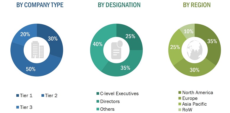
Wafer Cleaning Equipment Market Size, and Share

To know about the assumptions considered for the study, download the pdf brochure

Market Size Estimation

The top-down and bottom-up approaches have been used extensively in market engineering. Several data triangulation methods have also been used to perform market forecasting and estimation for the report’s overall market segments and sub-segments. Multiple qualitative and quantitative analyses have been performed on the market engineering process to gain key insights throughout the report.

Secondary research has been used to identify the key players offering wafer cleaning equipment. The revenues of those key players have been determined through both primary and secondary research. The revenues have been identified geographically as well as market segment-wise, using financial statements and analysing annual reports of the key market players. Interviews with CEOs, VPs, directors, and marketing executives have also been conducted to gain insights into the key players and the wafer cleaning equipment market. All the market shares have been estimated using secondary and primary research. This data has been consolidated, supplemented with detailed inputs and analysis from MarketsandMarkets, and presented in this report.

Market Size Estimation Methodology-Bottom-up Approach

The bottom-up approach has been employed to arrive at the overall size of the wafer cleaning equipment market from the calculations based on the revenues of the key players and their shares in the market. Key players in the wafer cleaning equipment market, including SCREEN Holdings Co., Ltd. (Japan), Tokyo Electron Limited (Japan), Applied Materials (US), LAM Research Corporation (US), and Entregris Inc., (US) have been studied. The market size estimations have been carried out considering the market size of their wafer cleaning equipment offerings.

Wafer Cleaning Equipment Market Size, and Bottom-up Approach

Market Size Estimation Methodology-Top-down Approach

In the top-down approach, the overall market size has been used to estimate the size of individual markets through percentage splits from secondary and primary research.
The most appropriate parent market size has been used to implement the top-down approach for the calculation of specific market segments.

The revenue shares used earlier in the bottom-up approach were verified by identifying and estimating the market share for each company. The overall parent market size and individual market sizes have been determined and confirmed in this study through the data triangulation process and data validation through the primaries.

Wafer Cleaning Equipment Market Size, and Top-down Approach

Data Triangulation

After arriving at the overall market size from the market size estimation process explained above, the total market has been then split into several segments and sub-segments. Data triangulation has been employed to complete the market engineering process and arrive at the exact statistics for all segments and sub-segments. The data has been triangulated by studying various factors and trends from both the demand and supply sides. Along with this, the market has been validated using both the top-down and bottom-up approaches.

Market Definition

A wafer stands as a slender piece of semiconductor material employed in electronics to create integrated circuits (ICs). These wafers consist of exceptionally pure and defect-free substances like silicon. Before integration into any device, these wafers necessitate chemical cleansing.

According to Shibaura Mechatronics Corporation, wafer cleaning equipment employs chemicals and pure water to meticulously eliminate dust and stains that could result in defects during the manufacturing of semiconductor wafers. Various varieties of wafer cleaning equipment are accessible in the market, including single wafer spray systems, single wafer cryogenic systems, batch immersion cleaning systems, batch spray cleaning systems, and scrubbers. The specific choice of wafer cleaning equipment hinges on factors like wafer size, the nature of contaminants and impurities, required throughput, and the arrangement of devices in which the wafers will be employed. This cleaning process reduces wafer impurities and enhances their suitability for semiconductor devices.

Among these, single wafer spray systems are anticipated to be the primary driver of market growth due to their extensive adoption within the semiconductor sector. These systems demonstrate considerable promise in purifying wafer surfaces with minimal damage. As the number of wafer cleaning steps expands, there's an increased demand for diverse wafer cleaning equipment, leading to the introduction of advanced cleaning technologies. The market's demand for wafer cleaning equipment is likely to experience fluctuations in the forthcoming years.

Key Stakeholders

  • Raw material and manufacturing equipment suppliers
  • Original equipment manufacturers (OEMs) (semiconductor device manufacturers)
  • ODMs and OEMs for semiconductor equipment
  • Research organizations
  • Organizations, forums, alliances, and associations based on technology standards
  • Technology investors
  • Governments, financial institutions, and investment communities
  • Analysts and strategic business planners
  • End users

The main objectives of this study are as follows:

  • To describe and forecast the wafer cleaning equipment market, by equipment type, application, and geography, in terms of value
  • To describe and forecast the wafer market, by wafer size, in terms of value and volume, and application, in terms of value
  • To describe technologies and processes used in wafer cleaning, as well as provide information on operating modes of wafer cleaning equipment
  • To describe sources and categories of impurities and their impact on wafers
  • To forecast the market size for various segments with regard to 3 main regions, namely, the Americas, EMEA, and Asia Pacific, in terms of value
  • To provide detailed information regarding major factors such as drivers, restraints, opportunities, and challenges influencing the growth of the market
  • To provide an overview of the value chain of the wafer cleaning equipment ecosystem and analyze market trends
  • To strategically analyze micromarkets1 with respect to individual growth trends, prospects, and contributions to the total market
  • To analyze opportunities in the market for various stakeholders by identifying high-growth segments of the wafer cleaning equipment market
  • To strategically profile the key players and comprehensively analyze their market position in terms of ranking and core competencies2, along with detailing the competitive landscape for market players
  • To analyze competitive developments such as collaborations, partnerships, mergers and acquisitions, new product launches and developments, business expansions, research and development in the wafer cleaning equipment market

Available Customizations

With the given market data, MarketsandMarkets offers customizations according to the specific requirements of companies. The following customization options are available for the report:

Country-wise Information:

  • Analysis for additional countries (up to five)

Company Information:

  • Detailed analysis and profiling of additional market players (up to five)
Custom Market Research Services

We will customize the research for you, in case the report listed above does not meet with your exact requirements. Our custom research will comprehensively cover the business information you require to help you arrive at strategic and profitable business decisions.

Request Customization
Report Code
SE 1235
Published ON
Aug, 2023
Choose License Type
BUY NOW
  • SHARE
X
Request Customization
Speak to Analyst
Speak to Analyst
OR FACE-TO-FACE MEETING
PERSONALIZE THIS RESEARCH
  • Triangulate with your Own Data
  • Get Data as per your Format and Definition
  • Gain a Deeper Dive on a Specific Application, Geography, Customer or Competitor
  • Any level of Personalization
REQUEST A FREE CUSTOMIZATION
LET US HELP YOU!
  • What are the Known and Unknown Adjacencies Impacting the Wafer Cleaning Equipment Market
  • What will your New Revenue Sources be?
  • Who will be your Top Customer; what will make them switch?
  • Defend your Market Share or Win Competitors
  • Get a Scorecard for Target Partners
CUSTOMIZED WORKSHOP REQUEST
+1-888-600-6441
  • Call Us
  • +1-888-600-6441 (Corporate office hours)
  • +1-888-600-6441 (US/Can toll free)
  • +44-800-368-9399 (UK office hours)
CONNECT WITH US
ABOUT TRUST ONLINE
©2024 MarketsandMarkets Research Private Ltd. All rights reserved
DMCA.com Protection Status Website Feedback