Patterning Material Market by Type (193 NM Immersion Resist, Positive 193 NM Dry Resist, Positive 248 NM Resist, I-Line and G-Line Resist, and Others), by Application (Automotive Sensors, DRAM, Glass Printed Circuit Boards, MEMS & NEMS Devices, and Others) - Regional Forecasts to 2020


The global patterning material market size in terms of value is projected to reach USD 3.86 billion by 2020, at a CAGR of 5.85% from 2015 to 2020. Patterning materials or photoresists are light sensitive materials used in the photolithography (device patterning process) processes to form patterned coating on a surface for wafers, usually silicon wafers, used in the electronics & semiconductors. Several chemicals such as polymethyl methacrylate (PMMA) and polymethyl glutarimide (PMGI), and novolac are also used to enhance the material property in the patterning process. Lights used to get the desired pattern print on the material are generally UV, Deep UV, and, i and g lines having wavelengths ranging from 350nm to 450nm. Exposure to the desired light wavelength induces photochemical reactions that change the solubility of the light-exposed area on the photoresist film resulting into pattern formation. The pattern is then imprinted on the wafer through etching process.
The major driving factors for the market are the rapidly growing Integrated Circuit (IC) market and technological advancement facilitating the era of nanodevices. The new era of miniaturized semiconductor devices also acts as growth driver for the photoresists market. The major challenge for the market is to encounter the cost-related problems associated with the lithography process. The major opportunities for the market are present in the developing economies that are expected to possess strong demand for electronic products such as mobile, tablets, and so on in the near future.
Market players have focus on enhancing their product portfolio through new product/technology development in the period from 2010 to 2015. Other development strategies adopted by market players are capacity expansions, agreements & collaborations, joint ventures, and mergers & acquisitions.
Scope of the Report
The report analyzes the patterning material market based on its types as per the specific light wavelength used in the patterning process, various applications, and covers the market demand in major regions. The report also provides a market overview for the patterning materials market.
By Type:
- I-line and g-line
- Positive 248nm
- Positive 193nm dry resist
- Positive 193nm immersion resist
- Others
By Application:
- DRAM
- Automotive sensors
- MEMS & NEMS Devices
- Glass Printed Circuit Boards
- Others
By Region:
- Asia-Pacific
- North America
- Europe
- RoW
This report also includes key participants in the patterning material market including Fujifilm Holding Corporation (Japan), JSR Micro Inc. (U.S.), Merck KGaA (Germany), Shin-etsu Chemical Co., Ltd. (Japan), and so on.
Patterning materials or photoresists are light sensitive materials used in the photolithography (device patterning process) processes to form patterned coating on a surface for wafers, usually silicon wafers, used in the electronics & semiconductors. Several chemicals such as polymethyl methacrylate (PMMA) and polymethyl glutarimide (PMGI), and novolac are also used to enhance the material property in the patterning process. Lights used to get the desired pattern print on the material are generally UV, Deep UV, and, i and g lines having wavelengths ranging from 350nm to 450nm. Exposure to the desired light wavelength induces photochemical reactions that change the solubility of the light-exposed area on the photoresist film resulting into pattern formation. The pattern is then imprinted on the wafer through etching process. The new era of miniaturized semiconductor devices acts as growth driver for the photoresists market.
The key types of photoresist used are positive 193nm immersion resist, positive 193 nm dry resist, positive 248nm resist, i-line & g-line resist, and others. The key applications of the photoresist include automotive sensors, DRAM, glass printed circuit boards, MEMS & NEMS devices, and others.
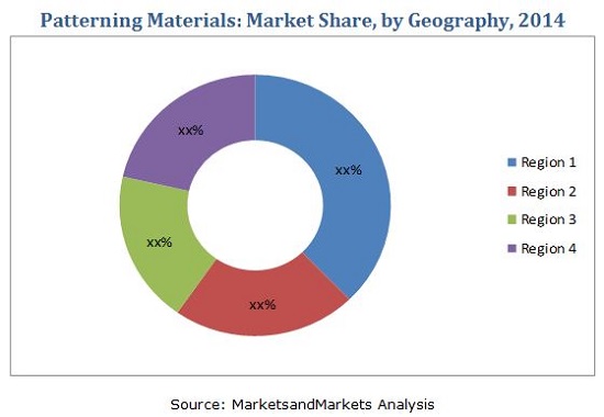
The total market size for patterning material is projected to reach USD 3,862.44 Million by 2020 from USD 2,750.00 Million in 2014, at a CAGR of 5.85% between 2015 and 2020. Globally, Asia-Pacific is projected to have the largest market size in terms of value as well as volume by 2020, followed by the North America region. Rest of the World (RoW) region is projected to be the fastest growing market, at a CAGR of 9.56%, by value, from 2015 to 2020, owing to rise in consumption in the region, where end-user markets for patterning materials is growing steadily in Brazil , Mexico. The European market for patterning materials is mature and is projected to grow at a rate of about 3.15% in terms of value.
The major driving factors for the market are the rapidly growing Integrated Circuit (IC) market and technological advancement facilitating the era of nanodevices. The major challenge for the market is to encounter the cost-related problems associated with the lithography process. The major opportunities for the market are present in the developing economies that are expected to possess strong demand for electronic products such as mobile, tablets, and so on in the near future.
Key participants in the patterning material market include Fujifilm Holding Corporation (Japan), JSR Micro Inc. (U.S.), Merck KGaA (Germany), Shin-etsu Chemical Co., Ltd., and so on. Market players concentrate on enhancing their product portfolio through new product/technology development. Other development strategies adopted by market players are capacity expansions, agreements & collaborations, joint ventures, and mergers & acquisitions.
The report analyzes the market on the basis of patterning material applications, introduction of photoresists/patterning materials in particular application in major regions, and also covers the market behavior of leading producers, key developments, and strategies implemented to sustain and succeed in the market.
 Exclusive indicates content/data unique to MarketsandMarkets and not available with any competitors.
Table of Contents
1 Introduction (Page No. - 15)
1.1 Objectives of the Study
1.2 Market Definition
1.3 Market Scope
1.3.1 Markets Covered
1.3.2 Years Considered for the Study
1.4 Currency & Pricing
1.5 Package Size
1.6 Limitations
1.7 Stakeholders
2 Research Methodology (Page No. - 18)
2.1 Research Data
2.1.1 Secondary Data
2.1.1.1 Key Data From Secondary Sources
2.1.2 Data From Primary Sources
2.1.2.1 Data From Primary Sources
2.1.2.2 Breakdown of Primary Interviews: By Company Type, Designation, and Region
2.2 Market Size Estimation
2.2.1 Bottom Up Approach
2.2.2 Top Down
2.3 Market Breakdown and Data Triangulation
2.4 Research Assumptions and Limitations
2.4.1 Assumptions
2.4.2 Limitations
3 Executive Summary (Page No. - 26)
4 Premium Insights (Page No. - 30)
4.1 Significant Market Opportunities for Patterning Materials
4.2 Lifecycle Analysis, By Region
5 Market Overview (Page No. - 34)
5.1 Introduction
5.2 Segmentation
5.3 Market Dynamics
5.3.1 Drivers
5.3.1.1 Boost in the IC Market Substantiating the Demand From Major Applications
5.3.1.2 Technological Advancements Providing A Shift Towards Nanodevices
5.3.2 Restraints
5.3.2.1 Crash in Disposable Income Plunging the Demand for Electronic Consumer Products
5.3.2.2 Limited Consumption for Patterning Materials and Taxation Policy in the Emerging Economies
5.3.3 Opportunities
5.3.3.1 Advancements in Patterning Materials Technologies
5.3.3.2 Emerging Economies
5.3.4 Challenges
5.3.4.1 Cost Associated With Patterning Materials
6 Industry Trends (Page No. - 41)
6.1 Introduction
6.2 Pricing Analysis
6.3 Value Chain Analysis
6.4 Strategic Benchmarking
6.4.1 Regional Integration & Product Enhancement
7 Patterning Material Market, By Type (Page No. - 45)
7.1 Introduction
7.2 I-Line and G-Line
7.3 Positive 248nm
7.4 Positive 193 NM Dry Resist
7.5 Positive 193 NM Immersion Resist
7.6 Others
8 Patterning Materials Market, By Application (Page No. - 56)
8.1 Introduction
8.2 Dynamic Random-Access Memory (DRam)
8.3 Automotive Sensors
8.4 Nems and Mems Devices
8.5 Glass Printed Circuit Board
8.6 Others
9 Patterning Material Market, By Region (Page No. - 68)
9.1 Introduction
9.2 North America
9.2.1 U.S.
9.2.2 Canada
9.3 Europe
9.3.1 Germany
9.3.2 U.K.
9.3.3 France
9.3.4 Others
9.4 Asia-Pacific
9.4.1 Taiwan
9.4.2 South Korea
9.4.3 Japan
9.4.4 China
9.4.5 Rest of Asia-Pacific
9.5 RoW
9.5.1 Mexico
9.5.2 Brazil
9.5.3 Others
10 Competitive Landscape (Page No. - 115)
10.1 Overview
10.2 Competitive Situation & Trends
10.2.1 New Product/Technology Developments
10.2.2 Capacity Expansion
10.2.3 Agreements/Collaborations
10.2.4 Joint Ventures and Mergers & Acquisitions
11 Company Profiles (Page No. - 121)
(Business Overview, Products & Services, Key Insights, Recent Developments, SWOT Analysis, MnM View)*
11.1 Introduction
11.2 Fujifilm Holdings Corporation
11.3 JSR Micro, Inc.
11.4 Dongjin Semichem Co., Ltd.
11.5 Honeywell Electronic Materials, Inc.
11.6 Shin-Etsu Chemical Co., Ltd.
11.7 The DOW Chemical Company
11.8 Tokyo Ohka Kogyo Co., Ltd. (Tok)
11.9 Sumitomo Chemicals Co., Ltd.
11.10 Merck KGAA
11.11 Microchem Corporation
11.12 Brewer Science, Inc.
*Details on Business Overview, Products & Services, Key Insights, Recent Developments, SWOT Analysis, MnM View Might Not Be Captured in Case of Unlisted Companies.
12 Appendix (Page No. - 152)
12.1 Discussion Guide
12.2 Introducing Rt: Real-Time Market Intelligence
12.3 Available Customizations
12.4 Related Reports
List of Tables (114 Tables)
Table 1 Ic Market Boost and Nanotechnological Advancements are Expected to Drive the Growth of the Patterning Material Market
Table 2 Crash in Disposable Income and Limited Consumption Restricts Patterning Material Market Growth
Table 3 Emerging Technologies and Emerging Economies Expected to Revive the Patterning Material Market in the Near Future
Table 4 Cost Associated With Patterning Materials Poses Challenge to the Growth of the Market
Table 5 Patterning Material Market Size, By Type, 2013�2020 (USD Million)
Table 6 Patterning Material Market Size, By Type, 2013�2020 (Kgals )
Table 7 I-Line and G-Line Market Size, By Region, 2013�2020 (USD Million)
Table 8 I-Line and G-Line Market Size, By Region, 2013�2020 (Kgals)
Table 9 Positive 248nm Market Size (USD Million), By Region, 2013�2020
Table 10 Positive 248nm Market Size, By Region, 2013�2020 (Kgals)
Table 11 Positive 193 NM Dry Resist Market Size, By Region, 2013�2020 (USD Million)
Table 12 Positive 193 NM Dry Resist Market Size, By Region, 2013�2020 (Kgals)
Table 13 Positive 193 NM Immersion Resist Market Size, By Region, 2013�2020 (USD Million)
Table 14 Positive 193 NM Immersion Resist Market Size, By Region, 2013�2020 (Kgals)
Table 15 Other Photoresists Market Size, By Region, 2013�2020 (USD Million)
Table 16 Other Photoresists Market Size, By Region, 2013�2020 (Kgals)
Table 17 Patterning Material Market Size, By Application, 2013�2020 (USD Million)
Table 18 Patterning Material Market Size, By Application, 2013�2020 (Kgals )
Table 19 Patterning Material Market Size in DRam, By Region, 2013�2020 (USD Million)
Table 20 Market Size in DRam, By Region, 2013�2020 (Kgals )
Table 21 Patterning Material Market Size in Automotive Sensors,By Region, 2013�2020 (USD Million)
Table 22 Market Size in Automotive Sensors, By Region, 2013�2020 (Kgals)
Table 23 Patterning Material Market Size in Nems and Mems Devices, By Regio, 2013�2020 (USD Million)
Table 24 Market Size in Nems and Mems Devices,By Region, 2013�2020 (Kgals)
Table 25 Patterning Material Market Size in Gpcb, By Region, 2013�2020 (USD Million)
Table 26 Market Size in Gpcb, By Region, 2013�2020 (Kgals)
Table 27 Market Size in Others, By Region, 2013�2020 (USD Million)
Table 28 Patterning Material Market Size in Others, By Region, 2013�2020 (Kgals)
Table 29 Market Size, By Region, 2013�2020 (USD Million)
Table 30 Market Size, By Region, 2013�2020 (Kgals)
Table 31 North America: Market Size, By Country, 2013�2020 (USD Million)
Table 32 North America: Market Size, By Country, 2013�2020 (Kgals)
Table 33 North America: Market Size, By Type, 2013�2020 (USD Million)
Table 34 North America: Patterning Material Market Size, By Type, 2013�2020 (Kgals)
Table 35 North America: Market Size, By Application, 2013�2020 (USD Million)
Table 36 North America: Market Size, By Application, 2013�2020 (Kgals)
Table 37 U.S.: Market Size, By Type, 2013�2020 (USD Million)
Table 38 U.S.: Market Size, By Type, 2013�2020 (Kgals)
Table 39 U.S.: Market Size, By Application, 2013�2020 (USD Million)
Table 40 U.S.: Market Size, By Application, 2013�2020 (Kgals)
Table 41 Canada: Market Size, By Type, 2013�2020 (USD Million)
Table 42 Canada: Patterning Material Market Size, By Type, 2013�2020 (Kgals)
Table 43 Canada: Market Size, By Application, 2013�2020 (USD Million)
Table 44 Canada: Market Size, By Application, 2013�2020 (Kgals)
Table 45 Europe: Market Size, By Country, 2013�2020 (USD Million)
Table 46 Europe: Market Size, By Country, 2013�2020 (Kgals)
Table 47 Europe: Patterning Material Market Size, By Type, 2013�2020 (USD Million)
Table 48 Europe: Market Size, By Type, 2013�2020 (Kgals)
Table 49 Europe: Market Size, By Application, 2013�2020 (USD Million)
Table 50 Europe: Market Size, By Application, 2013�2020 (Kgals)
Table 51 Germany: Market Size, By Type, 2013�2020(USD Million)
Table 52 Germany: Market Size, By Type, 2013�2020 (Kgals)
Table 53 Germany: Patterning Material Market Size, By Application, 2013�2020 (USD Million)
Table 54 Germany: Market Size, By Application, 2013�2020 (Kgals)
Table 55 U.K.: Market Size, By Type, 2013�2020 (USD Million)
Table 56 U.K.: Market Size, By Type, 2013�2020 (Kgals)
Table 57 U.K.: Market Size, By Application, 2013�2020 (USD Million)
Table 58 U.K.: Patterning Material Market Size, By Application, 2013�2020 (Kgals)
Table 59 France: Market Size, By Type, 2013�2020 (USD Million)
Table 60 France: Market Size, By Type, 2013�2020 (Kgals)
Table 61 France: Market Size, By Application, 2013�2020 (USD Million)
Table 62 France: Market Size, By Application, 2013�2020 (Kgals)
Table 63 Others: Patterning Material Market Size, By Type, 2013�2020 (USD Million)
Table 64 Others: Market Size, By Type, 2013�2020 (Kgals)
Table 65 Others: Market Size, By Application, 2013�2020 (USD Million)
Table 66 Others: Market Size, By Application, 2013�2020 (Kgals)
Table 67 Asia-Pacific: Patterning Material Market Size, By Country, 2013�2020 (USD Million)
Table 68 Asia-Pacific: Market Size, By Country, 2013�2020 (Kgals)
Table 69 Asia-Pacific: Market Size, By Type, 2013�2020 (USD Million)
Table 70 Asia-Pacific: Market Size, By Type, 2013�2020 (Kgals)
Table 71 Asia-Pacific: Market Size, By Application, 2013�2020 (USD Million)
Table 72 Asia-Pacific: Market Size, By Application, 2013�2020 (Kgals)
Table 73 Taiwan: Market Size, By Type, 2013�2020 (USD Million)
Table 74 Taiwan: Patterning Material Market Size, By Type, 2013�2020 (Kgals)
Table 75 Taiwan: Market Size, By Application, 2013�2020 (USD Million)
Table 76 Taiwan: Market Size, By Application, 2013�2020 (Kgals)
Table 77 South Korea: Market Size, By Type, 2013�2020 (USD Million)
Table 78 South Korea: Market Size, By Type, 2013�2020 (Kgals)
Table 79 South Korea: Patterning Material Market Size, By Application, 2013�2020 (USD Million)
Table 80 South Korea: Market Size, By Application, 2013�2020 (Kgals)
Table 81 Japan: Market Size, By Type, 2013�2020 (USD Million)
Table 82 Japan: Market Size, By Type, 2013�2020 (Kgals)
Table 83 Japan: Patterning Material Market Size, By Application, 2013�2020 (USD Million)
Table 84 Japan: Market Size, By Application, 2013�2020 (Kgals)
Table 85 China: Market Size, By Type, 2013�2020 (USD Million)
Table 86 China: Patterning Material Market Size, By Type, 2013�2020 (Kgals)
Table 87 China: Market Size, By Application, 2013�2020 (USD Million)
Table 88 China: Market Size, By Application, 2013�2020 (Kgals)
Table 89 Rest of Asia-Pacific: Market Size, By Type, 2013�2020 (USD Million)
Table 90 Rest of Asia-Pacific: Patterning Material Market Size, By Type, 2013�2020 (Kgals)
Table 91 Rest of Asia-Pacific: Market Size, By Application, 2013�2020 (USD Million)
Table 92 Rest of Asia-Pacific: Market Size, By Application, 2013�2020 (Kgals)
Table 93 RoW: Market Size, By Country, 2013�2020 (USD Million)
Table 94 RoW: Patterning Material Market Size, By Country, 2013�2020 (Kgals)
Table 95 RoW: Market Size, By Type, 2013�2020 (USD Million)
Table 96 RoW: Market Size, By Type, 2013�2020 (Kgals)
Table 97 RoW: Market Size, By Application, 2013�2020 (USD Million)
Table 98 RoW: Market Size, By Application, 2013�2020 (Kgals)
Table 99 Mexico: Market Size, By Type, 2013�2020 (USD Million)
Table 100 Mexico: Market Size, By Type, 2013�2020 (Kgals)
Table 101 Mexico: Market Size, By Application, 2013�2020 (USD Million)
Table 102 Mexico: Market Size, By Application, 2013�2020 (Kgals)
Table 103 Brazil: Market Size, By Type, 2013�2020 (USD Million)
Table 104 Brazil: Market Size, By Type, 2013�2020 (Kgals)
Table 105 Brazil: Market Size, By Application, 2013�2020 (USD Million)
Table 106 Brazil: Patterning Material Market Size, By Application, 2013�2020 (Kgals)
Table 107 Others: Market Size, By Type, 2013�2020 (USD Million)
Table 108 Others: Market Size, By Type, 2013�2020 (Kgals)
Table 109 Others: Market Size, By Application, 2013�2020 (USD Million)
Table 110 Others: Market Size, By Application, 2013�2020 (Kgals)
Table 111 New Product/Technology Developments, 201o�2015
Table 112 Capacity Expansions, 2010�2015
Table 113 Agreements & Collaborations, 2010�2015
Table 114 Joint Ventures and Mergers & Acquisitions, 2010�2015
List of Figures (49 Figures)
Figure 1 Patterning Material Market: Research Design
Figure 2 Market Size Estimation Methodology: Bottom-Up Approach
Figure 3 Market Size Estimation Methodology: Top-Down Approach
Figure 4 Data Triangulation
Figure 5 Other Types of Patterning Materials to Witness the Highest Cagr Between 2015 and 2020
Figure 6 Mems & Nems to Be the Fastest-Growing Application
Figure 7 Asia-Pacific Accounted for the Largest Market Share, By Value (2014)
Figure 8 North America Accounted for Largest Market Share in Automotive Sensors, the Largest Application Segment, By Volume (2014)
Figure 9 Asia-Pacific Accounted for Highest Market Size By Value in 2014 Whereas RoW Projected to Witness Highest Growth Rate Between 2015 and 2020
Figure 10 Attractive Opportunities in the Patterning Material Market
Figure 11 Automotive Sensors Was the Largest Application in the Patterning Material Market (2014)
Figure 12 RoW to Be the Fastest-Growing Region in Patterning Materials Market, By Value, Between 2015 and 2020
Figure 13 Others Sector to Be the Fastest-Growing Segment By Type Between 2015 and 2020
Figure 14 Asia-Pacific Accounted for the Largest Share in the Patterning Materials Market, By Value (2014)
Figure 15 The Asia-Pacific Market is in the Growth Stage
Figure 16 Patterning Materials: Market Dynamics
Figure 17 Patterning Materials: Pricing Analysis for Different Types
Figure 18 Patterning Materials: Value-Chain Analysis
Figure 19 Strategic Benchmarking: Major Companies Focusing on Agreements & Partnerships
Figure 20 Asia-Pacific Projected to Dominate the I-Line and G-Line Market Between 2015-2020 (USD Million)
Figure 21 Europe is Projected to Dominate the Positive 248nm Market Between 2015-2020
Figure 22 North America is Projected to Be the Largest Market for Positive 193 NM Dry Resist Between 2015-2020
Figure 23 Asia-Pacific is Projected to Be the Largest Market for Positive 193 NM Immersion Resist Between 2015-2020
Figure 24 Automotive Sensors are Projected to Account for the Largest Market Share By 2020 (USD Million)
Figure 25 North America to Be the Biggest Market for Patterning Material in DRam Application Between 2015 and 2020
Figure 26 North America Projected to Account for the Largest Market Share for Patterning Material in Automotive Sensors Between 2015 and 2020
Figure 27 North America to Account for the Largest Market Share in Nems and Mems Devices Application, 2015�2020
Figure 28 Asia-Pacific to Account for the Largest Market Share By 2020
Figure 29 Rapidly Growing Markets are Emerging as Strategic Destinations
Figure 30 Mems & Nems Devices is the Fastest-Growing Application, 2015�2020
Figure 31 China, Japan, and India are the Most Lucrative Markets
Figure 32 Companies Primarily Adopted Organic Growth Strategies Between 2010 and 2015
Figure 33 New Product/Technology Development Acted as the Key Strategy Adopted By Market Players
Figure 34 Battle for Market Share: New Product/Technology Development Was the Key Strategy
Figure 35 Regional Revenue Mix of Leading Market Players
Figure 36 Fujifilm Holdings Corporation: Company Snapshot
Figure 37 Fujifilm Holdings Corporation: SWOT Analysis
Figure 38 JSR Micro, Inc.: Company Snapshot
Figure 39 JSR Micro, Inc.: SWOT Analysis
Figure 40 Dongjing Semichem Co., Ltd.: SWOT Analysis
Figure 41 Honeywell Electronic Materials, Inc.: Company Snapshot
Figure 42 Honeywell Electronic Materials, Inc.: SWOT Analysis
Figure 43 Shin-Etsu Chemical Co., Ltd.: Company Snapshot
Figure 44 Shin-Etsu Chemical Co., Ltd: SWOT Analysis
Figure 45 The DOW Chemical Company: Company Snapshot
Figure 46 Tokyo Ohka Kogyo Co., Ltd.: Company Snapshot
Figure 47 Sumitomo Chemical Co., Ltd.: Company Snapshot
Figure 48 Merck KGAA: Company Snapshot
Figure 49 Merck KGAA: SWOT Analysis


Growth opportunities and latent adjacency in Patterning Material Market