
Silicon Photonics Market Size, Share, Trends and Growth

Silicon Photonics Market by Product (Transceivers, Variable Optical Attenuators, Switches, Sensors and Cables), Components (Lasers, Modulators, Optical Waveguides, Optical Interconnects, Photodetectors) - Global Forecast to 2030


OVERVIEW
Source: Secondary Research, Interviews with Experts, MarketsandMarkets Analysis
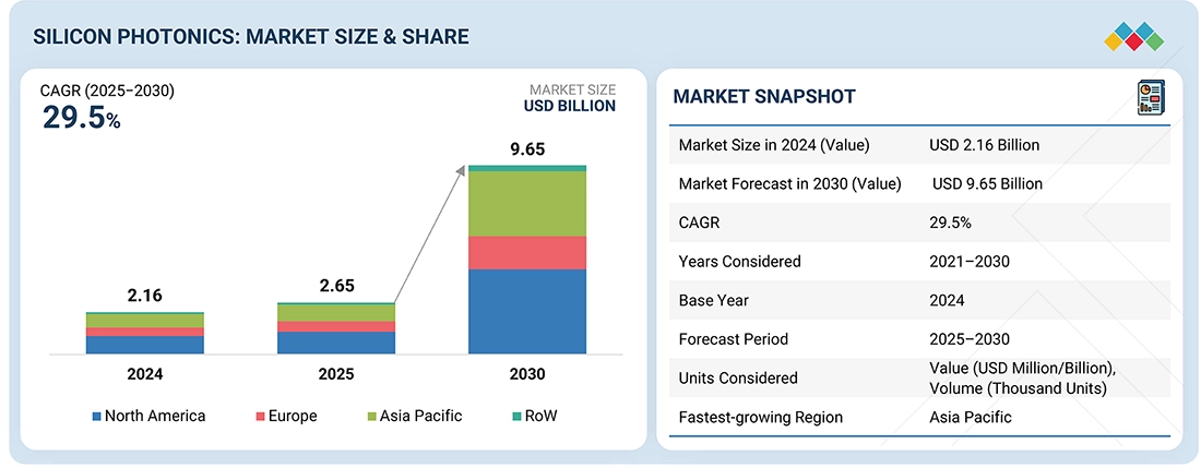
The silicon photonics market was valued at USD 2.16 billion in 2024 and is projected to reach USD 9.65 billion by 2030, growing at a CAGR of 29.5% from 2025 to 2030. Silicon photonics is experiencing strong growth due to the increasing demand for high-speed data transmission in AI, cloud computing, and quantum technologies. Trends indicate data centres, telecommunication, and healthcare are driving the adoption in a boom, and transceivers and high-performance computing (HPC) are the most positively affected positively.
KEY TAKEAWAYS
-
BY PRODUCTTransceivers are expected to have the largest market size during the forecast period. Transceivers are used in various end users, such as data centres and HPC, and telecommunications, owing to the growing need for high-speed data transmission in data center.
-
BY COMPONENTThe market for lasers is expected to grow at the highest CAGR during the forecast period. Lasers are an essential component in silicon photonics as they are used to generate and transmit light signals over long distances. The demand for high-speed data transmission and communication is expected to drive silicon photonics market growth, and lasers will play a critical role in enabling this technology
-
BY END USERThe data centers and HPC segment is projected to grow at the highest CAGR during the forecast period. WAN and LAN are used for metro and long-haul applications in telecommunications, and LAN is used in the data communication end-use segment.
-
BY REGIONNorth America is dominating the silicon photonics market by capturing the largest market share owing to the presence of major players providing silicon photonics technology-based devices in the US and the high adoption of electronic products.
-
COMPETITIVE LANDSCAPECisco Systems, Inc. (US), Intel Corporation (US), MACOM (US), GlobalFoundries Inc. (US), and Lumentum Operations LLC (US) are major players in the market. Major market players have adopted both organic and inorganic strategies, including partnerships and investments.
The silicon photonics market has been growing strongly as demands for high-bandwidth, low-latency and energy-efficient data communication increase. It is gradually shifting from niche applications into mainstream infrastructure, especially in data center, telecommunications, and AI/ML workloads where traditional copper interconnects are facing power, heat and speed limitations.
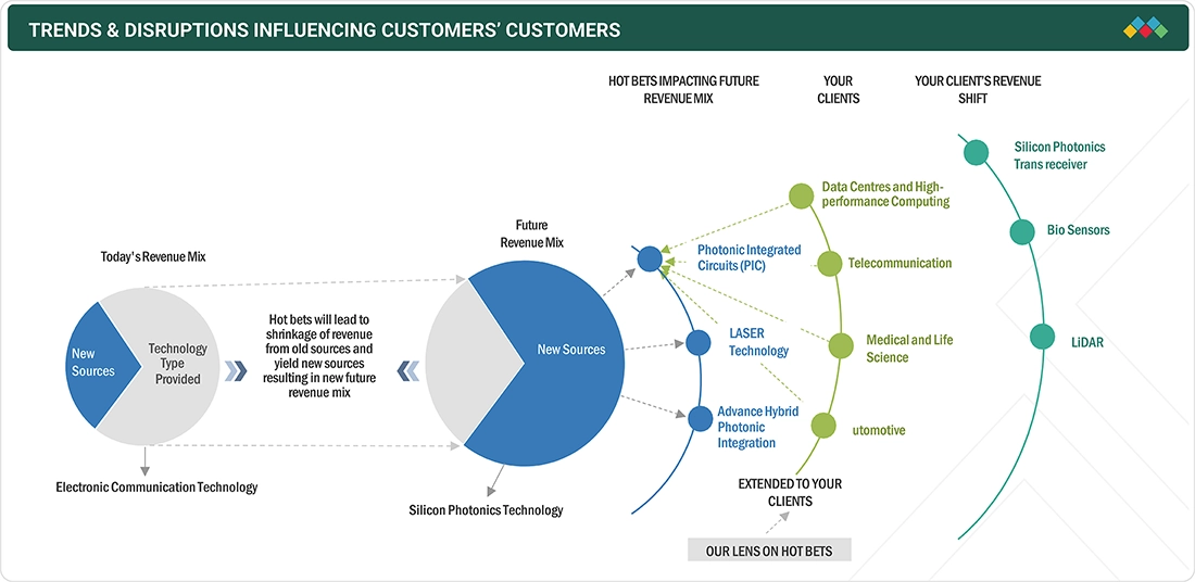
TRENDS & DISRUPTIONS IMPACTING CUSTOMERS' CUSTOMERS
The fig represents the revenue shift expected in the silicon photonics market. Communication is happening with electronic components, and electronic technology dominates in terms of value in the silicon photonics market. However, due to technological advancements, there is an increasing demand for high-speed data transmission in data centers and other applications, which is expected to lead to the rise of silicon photonics technology. Data centers, telecommunications, and medical and life sciences are a few industries that will experience a boost in market size. Silicon photonics transceivers, biosensors, and LIDAR demand will increase soon.
Source: Secondary Research, Interviews with Experts, MarketsandMarkets Analysis
MARKET DYNAMICS
Level
-
Growing need for high bandwidth and fast data transfer

-
Growing focus on energy efficiency and lower power costs

Level
-
Complexities associated with integrating on-chip lasers

Level
-
Ongoing advancements in quantum photonics

-
Expansion of 5G networks

Level
-
Rising thermal effects due to miniaturization of devices

-
Inefficient electroluminescence of bulk crystalline silicon

Source: Secondary Research, Interviews with Experts, MarketsandMarkets Analysis
Driver: Growing need for high bandwidth and fast data transfer
Rising volumes of streaming, cloud computing and AI workloads are pushing demand for data transfer capacities that far exceed what traditional copper interconnects can efficiently support. Silicon photonics offers a way out of this bottleneck by embedding optical components into silicon chips, enabling much faster and more energy-efficient data exchange, especially in hyperscale data centers and telecom networks. With roll-outs of 5G/6G, advances in photonic integration and economies of scale, the market for silicon photonics is accelerating rapidly as more sectors embrace high-speed, low-latency digital infrastructure.
Restraint: Ongoing advancements in quantum photonics
The integration of on-chip lasers remains a thorny technical hurdle for silicon photonics. Because silicon itself is an indirect bandgap material, it emits light poorly, so achieving efficient, reliable lasers on silicon requires incorporation of III-V semiconductors or complex hybrid techniques—with wafer bonding, flip-chip assembly or epitaxial growth—that complicate fabrication, raise costs and reduce yield. Further challenges like controlling thermal effects, managing reflections, ensuring accurate alignment, and keeping the process CMOS compatible all deepen the difficulty, so many commercial systems still rely on external lasers despite the loss of compactness, power savings, and full integration.
Opportunity: Rising thermal effects due to miniaturization of devices
Quantum photonics presents a powerful frontier for silicon photonics by enabling the generation, control, and manipulation of individual photons on a chip — critical for ultra-secure communications, quantum cryptography, and information processing. Researchers have recently shown progress in creating single-photon emitters in silicon (such as G and W centers) and designing microring or resonator-based sources with high spectral purity, which are steps toward integrating complex quantum circuits. Coupled with the use of mature CMOS-compatible manufacturing and foundry-scale production, these advances promise to bring quantum photonic systems out of the laboratory and into practical, scalable, high-performance applications.
Challenge: Rising thermal effects due to miniaturization of devices
As silicon photonics technology advances towards miniaturization and integration, thermal effects have become a significant challenge. The dense integration of components like modulators, waveguides, and detectors on a single chip leads to localized heating, which can alter the refractive index of silicon, resulting in signal drift, phase errors, or data loss. Unlike electronics, photonic devices are temperature-sensitive and require precise thermal management to maintain control and stability.
Silicon Photonics Market: COMMERCIAL USE CASES ACROSS INDUSTRIES
| COMPANY | USE CASE DESCRIPTION | BENEFITS |
|---|---|---|
 |
Data center optical transceivers and integrated optical interconnects for AI workloads | High-speed data transfer, reduced latency, improved energy efficiency, scalable optical I/O closer to CPU |
 |
High-speed optical interconnects integrated into networking equipment, enabled by Luxtera acquisition | Enhanced bandwidth for data centers and internet infrastructure, faster network speeds, improved network scalability |
 |
Silicon photonics-based optical components for telecom and hyperscale data communications | Enables high-capacity optical networking, lower power consumption, increased network reliability |
 |
Advanced silicon photonics in software-defined networking and high-speed switches | Improved network performance, efficient bandwidth management, agile data routing |
Logos and trademarks shown above are the property of their respective owners. Their use here is for informational and illustrative purposes only.
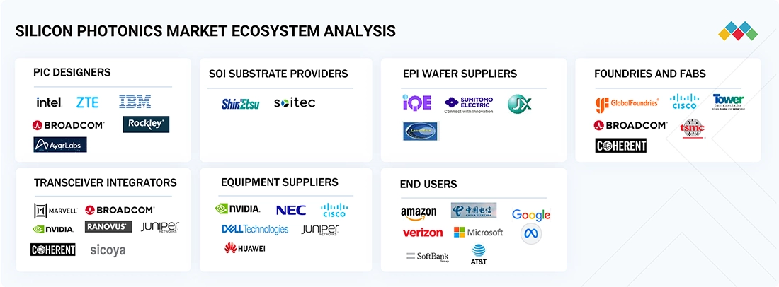
MARKET ECOSYSTEM
The silicon photonics ecosystem is characterized by photonic-integrated circuit (PIC) designers, silicon-on-insulator (SOI) substrate providers, epi wafer suppliers, foundries and fabs, transceiver integrators, equipment providers, and end users. PIC designers leverage SOI substrates and epi wafer technologies to integrate optical and electronic functions on a single chip. Foundries and fabs, such as GlobalFoundries and TSMC, play a crucial role by utilizing established semiconductor manufacturing processes to produce advanced PICS. Transceiver integrators incorporate essential optical components, such as modulators, detectors, and waveguides, onto a single silicon substrate. End users are from telecommunications, data centers, and HPC medical & life sciences fields.
Logos and trademarks shown above are the property of their respective owners. Their use here is for informational and illustrative purposes only.
MARKET SEGMENTS
Source: Secondary Research, Interviews with Experts, MarketsandMarkets Analysis
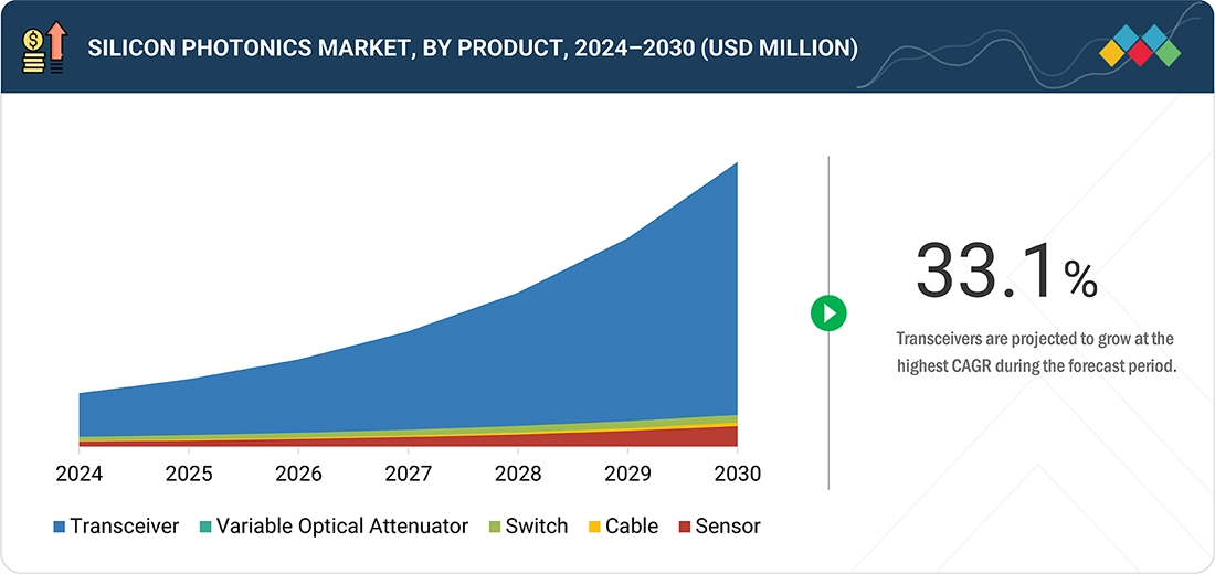
Silicon Photonics Market, By Produt Type
Transceiver in the product segment to hold largest market share throughout the forecast period.The transceiver industry is the largest in the silicon photonics industry primarily due to its inherent role in delivering high-speed data transmission in high-performance computing, telecommunications, and data centers. Silicon photonic transceivers offer several benefits over traditional electronic transceivers, including higher bandwidth, lower latency, and lower power consumption, that are critical in meeting the rising demand for higher speed and efficient data transmission
Silicon Photonics Market, By Component
Optical interconnects to have the highest CAGR during the forecast period. An optical interconnect is a technology that uses light (photons) transmitted through silicon-based waveguides to transfer data between different parts of an electronic system, such as between chips, servers, or data centers. Unlike traditional electrical interconnects that rely on copper wires to transmit electrical signals, optical interconnects use light, enabling faster and more energy-efficient data transfer with minimal signal loss over long distances.
Silicon Photonics Market, By End User
Data Centers and HPC are expected to have the highest growth rate during the forecast period.Data Centers and HPC include end users such as data centers and HPC Trans receivers, 5G trans receivers, photo processing, CPO, and optical interconnect. A data center and HPC is a facility consisting of networked computers and storage systems that many organizations use to organize, process, store, and disseminate large volumes of data. Businesses rely heavily on services, end users, and data in data centers, making it a critical asset for day-to-day operations.
REGION
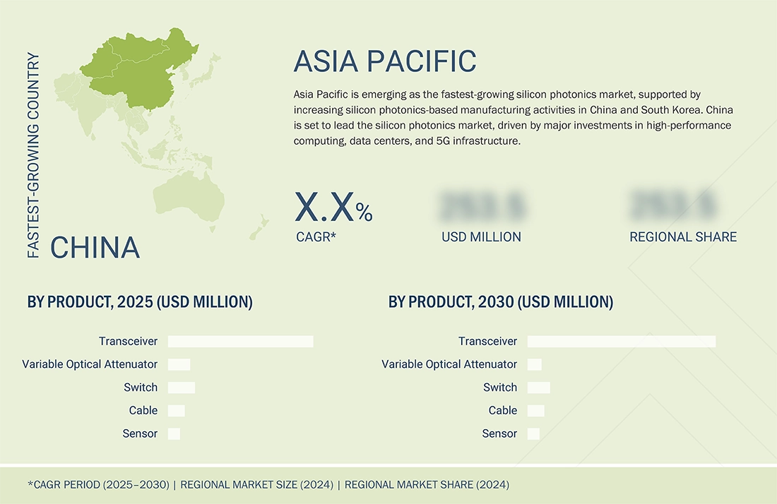
Asia Pacific to be fastest-growing region in global silicon photonics market during forecast period
The silicon photonics industry in Asia Pacific is expected to grow at the highest rate during the forecast period. The market in Asia Pacific has been segmented into China, Japan, South Korea, and Rest of Asia Pacific. The Rest of Asia Pacific mainly includes India, Australia, New Zealand, Singapore, Malaysia, the Philippines, and Taiwan. China is to record the largest market size within the silicon photonics industry, with revenue forecast to The fast-paced growth is powered by China's aggressive investment in high-performance computing, data centers, and 5G infrastructure, which represent key applications of silicon photonics technology.
The silicon photonics market in North America is projected to reach USD 4.35 billion by 2030, up from USD 1.16 billion in 2030, at a CAGR of 30.2% from 2025 to 2030. Silicon photonics is gaining significant momentum in North America as technology companies and data-center operators increasingly adopt high-speed, low-power optical connectivity. The region benefits from a mature semiconductor ecosystem, substantial R&D investments, and early adoption of AI and cloud computing workloads. Its expanding integration into applications like telecom networks, HPC systems, and advanced sensing further drives market growth.
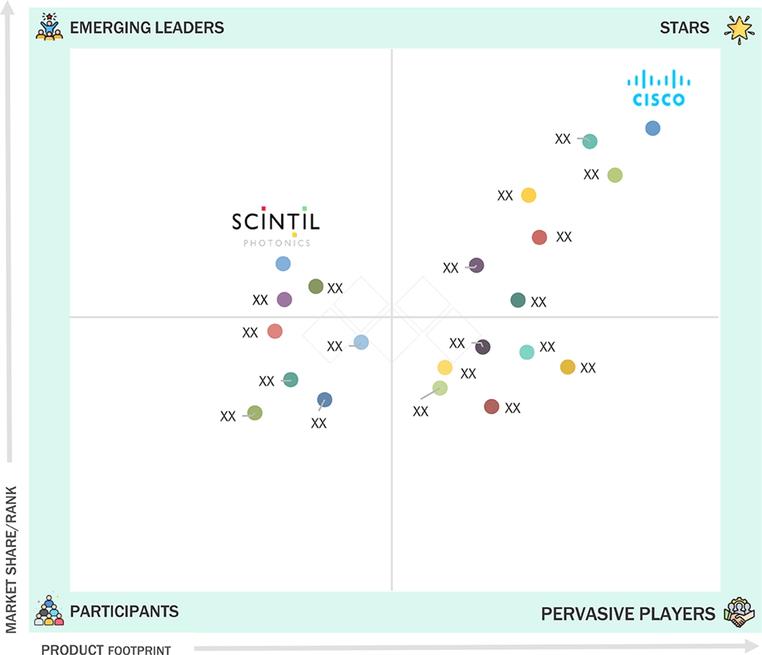
Silicon Photonics Market: COMPANY EVALUATION MATRIX
Star companies generally receive high scores for most evaluation criteria. They have a robust product portfolio, strong market presence, high market share, and effective business strategies. Major star companies in the silicon photonics market are Cisco Systems, Inc. (US). Players categorized as emerging leaders are the vendors who have demonstrated substantial product innovations compared to their competitors. These players mainly depend on investments and funding from other companies. SCINTIL Photonics (France) falls under this category.
Source: Secondary Research, Interviews with Experts, MarketsandMarkets Analysis
KEY MARKET PLAYERS
MARKET SCOPE
| REPORT METRIC | DETAILS |
|---|---|
| Market Size, 2024 (Value) | USD 2.16 Billion |
| Market Forecast, 2030 (Value) | USD 9.65 Billion |
| Growth Rate | CAGR of 29.5% from 2025 to 2030 |
| Years Considered | 2022–2030 |
| Base Year | 2024 |
| Forecast Period | 2025–2030 |
| Units Considered | Value (USD Million/Billion), Volume (Thousand Units) |
| Report Coverage | Revenue Forecast, Company Ranking, Competitive Landscape, Growth Factors, and Trends |
| Segments Covered |
|
| Regions Covered | North America, Asia Pacific, Europe, Rest of the World (RoW) |
WHAT IS IN IT FOR YOU: Silicon Photonics Market REPORT CONTENT GUIDE
DELIVERED CUSTOMIZATIONS
We have successfully delivered the following deep-dive customizations:
| CLIENT REQUEST | CUSTOMIZATION DELIVERED | VALUE ADDS |
|---|---|---|
| Data Center/Hyperscale OEM |
|
|
| Photonics Component Manufacturer |
|
Pinpoint highest-growth applications, address integration |
| Defense & Government Programs |
|
|
RECENT DEVELOPMENTS
- December 2024 : IBM (US) unveiled a new process for CPO that would enhance data center connectivity by integrating optical waveguides with silicon photonics. This technology was designed to replace traditional electrical interconnects, potentially speeding up data center training for generative AI models by up to five times. The use of polymer optical waveguides (PWGs) allowed for a higher density of optical fibers, up to six times more at the chip edge, improving bandwidth significantly and extending cable lengths from one meter to hundreds of meters.
- November 2024 : Celestial AI (US) acquired Rockley Photonics' (US) silicon photonics intellectual property (IP) portfolio for USD 20 million. This acquisition included worldwide issued and pending patents related to optoelectronic systems-in-package, electro-absorption modulators (EAMs), and optical switch technology. The integration of Rockley's IP enhanced Celestial AI's Photonic Fabric technology platform, which targeted AI data center infrastructure applications.
- October 2024 : Lumentum (US) participated in the European Conference on Optical Communication (ECOC) 2024, highlighting its enhanced 800G ZR+ coherent pluggable transceivers. These transceivers were optimized for extended reach and higher optical power applications, addressing the growing demands of AI infrastructure and long-reach data center interconnects. The transceivers leveraged Lumentum's proprietary indium phosphide technology for superior performance.
- March 2024 : MACOM (US) launched MACOM PURE DRIVE 200 Gbps per lane Liner Drive to enable the development of 1.6 TB linear pluggable optical (LPO) modules.
Table of Contents
 Exclusive indicates content/data unique to MarketsandMarkets and not available with any competitors.
Methodology
The study involved four major activities in estimating the current size of the silicon photonics market—exhaustive secondary research collected information on the market and its peer and parent markets. The next step was to validate these findings, assumptions, and sizing with industry experts across the value chain through primary research. Both top-down and bottom-up approaches were employed to estimate the total market size. After that, market breakdown and data triangulation were used to estimate the market size of segments and subsegments.
Secondary Research
Various secondary sources have been referred to in the secondary research process to identify and collect important information for this study. These secondary sources include silicon photonics technology journals and magazines, annual reports, press releases, investor presentations of companies, white papers, certified publications and articles from recognized authors, and directories and databases such as Factiva, Hoovers, and OneSource.
Primary Research
Various primary sources from the supply and demand sides have been interviewed in the primary research process to obtain qualitative and quantitative information important for this report. The primary sources from the supply side included industry experts such as CEOs, VPs, marketing directors, technology and innovation directors, and related executives from key companies and organizations operating in the silicon photonics market. After complete market engineering (including calculations regarding market statistics, market breakdown, market size estimations, market forecasting, and data triangulation), extensive primary research was conducted to gather information as well as to verify and validate the critical numbers arrived at.

Note: Other designations include sales, marketing, and product managers. Tier 1 = USD 1 billion, Tier 2 = USD 0.5–1.0 billion, and Tier 3 = USD 0.5 billion.
To know about the assumptions considered for the study, download the pdf brochure
Market Size Estimation
In the complete market engineering process, top-down and bottom-up approaches and several data triangulation methods have been implemented to estimate and validate the size of the silicon photonics market and other dependent submarkets listed in this report.
- Extensive secondary research has identified key players in the industry and market.
- In terms of value, the industry’s supply chain and market size have been determined through primary and secondary research processes.
- All percentage shares, splits, and breakdowns have been determined using secondary sources and verified through primary sources.
Silicon Photonics Market : Top-Down and Bottom-Up Approach

Data Triangulation
After arriving at the overall market size from the estimation process explained above, the global market has been split into several segments and subsegments. Market breakdown and data triangulation procedures have been employed wherever applicable to complete the overall market engineering process and arrive at exact statistics for all segments and subsegments. The data has been triangulated by studying various factors and trends identified from both the demand and supply sides.
Market Definition
Silicon photonics is a technique that employs semiconductor-grade silicon to integrate photonic circuits and electronic components on a single microchip. This method minimizes system power consumption while increasing transmission bandwidth by employing silicon as an optical medium. Instead of electrical impulses, the technology transfers data using optical beams, which may send enormous amounts of data at a faster rate than electrical signals.
Key Stakeholders
- Component and material providers
- Semiconductor foundries
- Silicon photonics platform developers
- Silicon photonics product manufacturers and suppliers
- Assembly and testing vendors
- Original equipment manufacturers
- Research organizations and consulting companies
- Technology investors
- Associations, alliances, and organizations related to silicon photonics
- Analysts and strategic business planners
- End users
Report Objectives
- To describe and forecast the silicon photonics market size, in terms of value, by product, component, end user, and region
- To describe and forecast the market size across four key regions, namely, North America, Europe, Asia Pacific, and the Rest of the World (RoW), along with their respective country-level market size, in terms of value
- To provide details regarding the silicon photonic waveguide range
- To provide detailed information regarding the drivers, restraints, opportunities, and challenges of the silicon photonics market
- To strategically analyze the micromarkets1 concerning the individual growth trends, prospects, and their contribution to the silicon photonics market
- To map competitive intelligence based on company profiles, key player strategies, and key developments
- To provide a detailed overview of the silicon photonics value chain and ecosystem
- To provide information about the key technology trends and patents related to the silicon photonics market
- To provide information regarding trade data related to the silicon photonics market
- To analyze opportunities in the market for stakeholders by identifying high-growth segments of the silicon photonics ecosystem
- To benchmark the market players using the proprietary company evaluation matrix framework, which analyzes them on various parameters within the broad categories of market ranking/share and product portfolio
- To analyze competitive developments such as contracts, acquisitions, product launches and developments, collaborations, and partnerships, along with research & development (R&D), in the silicon photonics market
- To analyze the impact of the recession on the growth of the silicon photonics market
Available Customizations
With the given market data, MarketsandMarkets offers customizations according to a company’s specific needs. The following customization options are available for the report:
Company Information:
- Detailed analysis and profiling of additional market players (up to 5)
Key Questions Addressed by the Report
Need a Tailored Report?
Customize this report to your needs
Get 10% FREE Customization
Customize This ReportPersonalize This Research
- Triangulate with your Own Data
- Get Data as per your Format and Definition
- Gain a Deeper Dive on a Specific Application, Geography, Customer or Competitor
- Any level of Personalization
Let Us Help You
- What are the Known and Unknown Adjacencies Impacting the Silicon Photonics Market
- What will your New Revenue Sources be?
- Who will be your Top Customer; what will make them switch?
- Defend your Market Share or Win Competitors
- Get a Scorecard for Target Partners

Custom Market Research Services
We Will Customise The Research For You, In Case The Report Listed Above Does Not Meet With Your Requirements
Get 10% Free CustomisationGrowth opportunities and latent adjacency in Silicon Photonics Market


VITTORIO
Oct, 2009
Dear Team Members, as an interviewed expert for this matter, I ask you to receive a PDF copy of the summary for this report. .
Angelica
Jan, 2019
I work in the field of silicon photonics components, and I am interested in receiving report specifically mentioning the market size for sensing component and automotive end user vertical. .
richard
Dec, 2009
Interested in silicon photonics market. Your report may receive beneficial publicity in a feature that I am due to write very soon. But I need free access for a limited period for this to happen..
richard
Mar, 2015
Need information on silicon photonic companies and their business models - service or product oriented ? .
Rapha�l
Sep, 2019
My objective is to assess the market in which I'll soon work into, see which business segment is likely to grow the most, and how fast?.
Suzanne
Aug, 2018
Dear sir/madam, just a quick question about the report. We would like to know if we are mentioned in this report. Could you provide me with that information? .
Jeremy
Aug, 2011
I'm a student interested in photonics and learning about the field and what opportunities there are within it. I'm interested in the building blocks of silicon photonics, silicon photonics technology trends, a general market overview. I'm also interested in silicon optical interconnects and photovoltaics, as well as information on HP, Intel, Oracle, and Translucent. .
Yung
Mar, 2019
As an optical engineer, I am very much interested in the market of SIP. I believe this report can help us to analyze that if it is worth to develop the SIP in our own company..
Giuseppe
Feb, 2014
Need information on Silicon Photonics Market by Products (Silicon Optical Interconnects & Wavelength Division Multiplexer Filters & Others), Applications (Telecommunication, Datacom, High Performance Computing & Others) & Geography - Analysis & Forecast (2013 - 2020)..
Jaci
Jun, 2010
We are looking for the following on the Overall Photonics Market: market size, market growth, major players, various segments within Photonics (& their relative sizes and growth)..
Carlos
Nov, 2018
Hello, I would like to buy the corporate license of the silicon photonics report so that I can share it with all the members of our association. I am interested in acquiring 3-6 reports per year from you..
Linda
Oct, 2015
I would like to obtain an old report on this topic from 2010-2014 for research purposes. .
Sevil
Oct, 2022
I need this analysis in order to make an impactful presentation and a review paper on silicon photonics. .
Christian
Jul, 2015
My group is working in the area of silicon photonics and integrated optics, and we are analyzing the potential of commercializing our research. To this end, a copy of the report of an executive summary would be extremely helpful. .
Rudy
Jan, 2019
Objective is to obtain a better market picture of how silicon photonics technology will impact fiber data center links..