AI Semiconductor Manufacturing Equipment Market 2032: Size, Share & Growth Report


The AI semiconductor manufacturing equipment market reached an estimated USD 53,915.7 million in 2025 and is projected to climb to USD 172,768.5 million by 2032, expanding at a CAGR of 18.1% from 2026 to 2032. The catalyst is a multi-year fab expansion cycle driven by a single force: the world needs more AI chips than the current manufacturing base can produce, and building the fabs to close that gap requires tens of billions of dollars in equipment. Front-end fab equipment investment reached an estimated USD 110 billion globally in 2025 and is forecast to grow 18% in 2026 to roughly USD 126 billion, with AI-related capacity accounting for the fastest-growing share. Every leading-edge AI chip—NVIDIA's Blackwell, AMD's MI400, Google's TPU Ironwood, Amazon's Trainium3—fabricates on TSMC's most advanced nodes using equipment that only five companies in the world can supply: ASML for lithography, Applied Materials for deposition, Tokyo Electron for multi-process platforms, Lam Research for etch, and KLA for metrology. These five firms are the structural bottleneck and the structural beneficiary of the AI buildout, and the market for the equipment they manufacture is expanding at a pace driven not by cyclical demand but by the construction of an entirely new tier of semiconductor infrastructure.
Top 10 Key Takeaways
- Asia Pacific holds the largest regional base by a wide margin, as Taiwan, South Korea, China, and Japan consume over 70% of global semiconductor equipment.
- North America is the fastest-growing major region, propelled by CHIPS Act-funded fab construction on US soil.
- Lithography (EUV / High-NA EUV) is the highest-value equipment category, with a single EUV system costing USD 150–350 million.
- Advanced packaging equipment (CoWoS, hybrid bonding, TSV) is the fastest-growing category, driven by the HBM and chiplet revolution.
- Leading-edge logic fabs (3nm and below) are the largest end-use fab type, while advanced memory fabs (HBM, advanced DRAM) are the fastest-growing.
- Five companies—ASML, Applied Materials, Tokyo Electron, Lam Research, and KLA—control the critical path for every AI chip manufactured on the planet.
- ASML's monopoly on EUV lithography makes it the single most strategically important equipment company; its High-NA EUV achieved "first light" for sub-2nm production.
- Export controls restricting equipment sales to China have created two parallel equipment markets and reshaped global trade flows.
- The near-term opportunity lies in CHIPS Act fab equipment orders, advanced packaging capacity expansion, and AI-driven smart manufacturing within fabs.
- The near-term risk is EUV lead times stretching to 18–24 months, workforce scarcity for equipment installation, and the geopolitical fragmentation of the semiconductor supply chain.
Why the AI Semiconductor Manufacturing Equipment Market Matters Now
Every AI chip starts as a bare silicon wafer and ends as a packaged processor through a sequence of hundreds of manufacturing steps, each performed by a specialized machine. The lithography tools that pattern circuits at nanometer scale, the deposition systems that build layers atom by atom, the etch tools that carve those patterns into silicon, the metrology systems that measure and inspect at every step, and the packaging equipment that stack HBM and assemble chiplets—these machines are the physical infrastructure of the AI revolution. Without them, no AI chip gets made. The market for this equipment is expanding because the world is building more fabs, at more advanced nodes, in more countries than at any point in semiconductor history.
The market covers the manufacturing equipment purchased by semiconductor fabs to produce AI-optimized chips—including GPUs, custom ASICs, HBM, and the advanced packaging that integrates them. It includes front-end wafer-processing equipment (lithography, deposition, etch, metrology, ion implantation, CMP, cleaning), back-end assembly and packaging equipment (CoWoS, hybrid bonding, TSV, die bonding, wire bonding), and test and probe equipment. It spans equipment used in leading-edge logic fabs (TSMC, Samsung, Intel), advanced memory fabs (SK Hynix, Samsung, Micron), advanced packaging and OSAT facilities, and the mature-node fabs that produce automotive and IoT chips alongside AI support components.
Three forces are converging to sustain multi-year demand. First, the leading-edge node migration—from 3nm to 2nm to angstrom-class nodes (TSMC A14, A16, Intel 18A)—requires new-generation equipment at each step, as the physics of smaller transistors demands more EUV layers, more precise deposition, and more advanced metrology. Second, the HBM and advanced packaging capacity buildout is creating an entirely new equipment demand pool, as fabs invest in CoWoS, hybrid bonding, and TSV tools to assemble the memory stacks and chiplet packages that AI accelerators require. Third, sovereign fab programs—the CHIPS Act in the US, the EU Chips Act, and national programs in Japan, South Korea, India, and the Middle East—are building greenfield fabs that must be equipped from scratch, creating parallel demand pools in geographies that previously imported finished chips rather than manufactured them. This market connects to the [INTERNAL LINK: AI accelerator market], the [INTERNAL LINK: semiconductor advanced packaging market], and the [INTERNAL LINK: high-bandwidth memory market].
Market Trends Shaping AI Semiconductor Manufacturing Equipment
The defining trend is AI as both the demand driver and the manufacturing enabler. AI chip demand is filling fabs and driving equipment orders, while AI is simultaneously being deployed inside the fabs themselves: AI-driven process optimization has demonstrated up to 57x simulation acceleration for high-NA EUV and angstrom-level processes, AI-powered defect detection is improving yield, and machine-learning-based predictive maintenance is increasing equipment uptime. The equipment vendors themselves are embedding AI into their platforms—ASML's EUV systems use AI for source-power optimization, and Applied Materials uses AI-driven computational modeling across its deposition portfolio.
A second trend is the EUV-to-High-NA-EUV lithography inflection. ASML's High-NA EUV system achieved "first light" in February 2024, and in 2026 the company increased EUV source power to 1,000 watts, lifting throughput. High-NA EUV is essential for sub-2nm nodes—without it, chipmakers cannot pattern the features required for next-generation AI processors. A single High-NA EUV system reportedly costs over USD 350 million, and the order pipeline for these machines is the most supply-constrained segment of the equipment market.
A third trend is advanced packaging equipment becoming a market unto itself. The HBM revolution and the shift toward chiplet architectures have made CoWoS, hybrid bonding, and TSV equipment the fastest-growing category. TSMC is expanding CoWoS capacity aggressively, and equipment suppliers are scaling packaging tool production to meet demand that was negligible five years ago. Advanced packaging equipment revenue is growing faster than any front-end category.
A fourth trend is sovereign fab programs creating parallel equipment demand pools. The CHIPS Act is funding over USD 50 billion in US fab construction—TSMC's USD 65 billion Arizona complex, Intel's Ohio and Oregon expansions, Samsung's Taylor, Texas fab, Micron's New York facility. The EU Chips Act supports Intel's EUR 33 billion Magdeburg complex and other European fabs. Japan's Rapidus installed its first production EUV tool in December 2024. Each greenfield fab must be equipped from scratch, creating demand that is additive to the ongoing replacement and upgrade cycle in existing fabs.
A fifth trend is China's domestic equipment ecosystem under export controls. Restricted from purchasing the most advanced equipment from ASML, Applied Materials, Lam Research, and others, Chinese fabs are investing in domestic alternatives from NAURA, AMEC, and ACM Research. This parallel ecosystem is growing rapidly from a low base but remains generations behind the leading edge, creating a bifurcated market where China consumes large volumes of mature-node equipment while the rest of the world races ahead on EUV and High-NA EUV.
Market Drivers Accelerating Growth
The first driver is AI chip demand driving multi-year fab expansion. Every major foundry and memory manufacturer is investing in new capacity to produce AI accelerators and HBM, and each new fab requires billions of dollars in equipment. This is not a one-quarter surge—it is a multi-year construction cycle that translates into sustained equipment demand.
The second driver is leading-edge node migration requiring new-generation equipment. The transition from 3nm to 2nm to angstrom-class nodes adds EUV patterning layers, introduces gate-all-around (GAA) transistor architectures that need new deposition and etch tools, and demands metrology systems capable of measuring features at atomic scale. Each node transition is an equipment-replacement event for the most critical process steps.
The third driver is HBM and advanced packaging capacity expansion. HBM production consumes roughly three times the wafer area per gigabyte versus DDR5, and the packaging of HBM stacks onto AI accelerators requires CoWoS tools, hybrid bonding systems, and TSV processing equipment. The explosion of HBM demand has created an entirely new equipment market that barely existed five years ago.
A fourth driver is CHIPS Act and sovereign fab investment creating greenfield demand. Fabs being built on US, European, and Japanese soil must be equipped from scratch, and the equipment orders for these greenfield facilities are additive to the ongoing demand from existing fabs in Taiwan, South Korea, and China.
Market Challenges and Restraints
The most significant restraint is ASML's monopoly on EUV lithography creating a single-point-of-failure supply constraint. ASML is the sole manufacturer of EUV and High-NA EUV systems, and its annual production capacity is limited to roughly 50–60 EUV units. Every leading-edge AI chip in the world depends on these machines, and any disruption to ASML's production—geopolitical, logistical, or technical—would ripple through the entire semiconductor industry.
A second restraint is export controls restricting equipment sales to China. US, Dutch, and Japanese export rules prevent the sale of the most advanced lithography, deposition, and etch tools to Chinese customers, shrinking a market that was historically one of the largest equipment-consuming regions. For equipment vendors, the lost China revenue is partially offset by demand elsewhere, but the geopolitical fragmentation adds compliance cost and operational complexity.
A third challenge is equipment lead times. EUV systems carry lead times of 18–24 months from order to delivery, and other leading-edge tools are not far behind. Fabs that need equipment urgently—to meet AI chip demand—face a queue that cannot be shortened by paying more.
Finally, workforce scarcity for equipment installation and maintenance is a real constraint. Installing and calibrating a High-NA EUV system requires ASML engineers who are in short supply, and the CHIPS Act fabs being built in the US face a shortage of trained technicians for every equipment category, not just lithography.
Segment Insights
By Equipment Type
Lithography (EUV / High-NA EUV / DUV) is the highest-value equipment category, as lithography tools are the most expensive machines in the fab—a single EUV unit costs USD 150–200 million, and a High-NA EUV system reportedly exceeds USD 350 million. ASML's lithography revenue accounts for roughly a quarter of total global equipment sales.
Advanced packaging equipment (CoWoS, hybrid bonding, TSV) is the fastest-growing category, driven by the HBM revolution and chiplet architectures that demand packaging tools at a scale and sophistication that the market has never seen.
By End-Use Fab Type
Leading-edge logic fabs (3nm and below) are the largest end-use category, as TSMC, Samsung, and Intel invest in capacity for AI GPUs and custom ASICs.
Advanced memory fabs (HBM, advanced DRAM) are the fastest-growing, as SK Hynix, Samsung, and Micron expand HBM production and invest in new DRAM process nodes to serve AI accelerator demand.
By Process Node
3nm is the current volume leader for leading-edge equipment, as every flagship AI chip fabricates on TSMC N3. 2nm and below is the fastest-growing node, as TSMC, Samsung, Intel, and Rapidus prepare production lines for the next generation.
Key segmentation conclusions:
- Lithography leads by value; advanced packaging equipment grows fastest.
- Leading-edge logic fabs anchor demand; advanced memory fabs grow fastest on HBM expansion.
- 3nm is the current volume node; 2nm and below is the fastest-growing as the next node transition begins.
- Five companies control the critical equipment path; ASML's EUV monopoly defines the supply ceiling.
- Sovereign fab programs are creating greenfield demand pools in geographies that previously had none.
Regional Analysis: AI Semiconductor Manufacturing Equipment Market by Region
Asia Pacific
Asia Pacific holds the largest base by a wide margin, valued at roughly USD 38,819.3 million in 2025 and projected to reach about USD 120,000.0 million by 2032, growing at a CAGR of 17.5%. Taiwan is the epicenter: TSMC alone accounts for the largest single share of global equipment purchases, and the island hosts the most advanced fabs in the world. South Korea is the second-largest buyer, driven by SK Hynix's and Samsung's HBM and advanced DRAM expansions—SK Hynix recently committed USD 8 billion in future technology investment with ASML for EUV-based AI chip production. China remains a large equipment market for mature-node tools despite export restrictions on leading-edge equipment, and domestic equipment makers (NAURA, AMEC) are scaling to fill the gap. Japan contributes through both domestic fab investment (Rapidus, TSMC Kumamoto) and as a major equipment-supplier base (Tokyo Electron, Advantest, SCREEN).
North America
North America is the fastest-growing major region, valued at roughly USD 7,548.2 million in 2025 and projected to reach about USD 28,000.0 million by 2032, growing at a CAGR of 20.6%. The CHIPS Act is the catalyst: TSMC's USD 65 billion Arizona complex, Intel's Ohio and Oregon fab expansions, Samsung's Taylor, Texas facility, and Micron's New York fab are all greenfield projects that must be equipped from scratch. The United States also hosts Applied Materials, Lam Research, KLA, and Axcelis—major equipment suppliers whose domestic proximity to these new fabs is a logistical and service advantage. The scale of CHIPS Act-funded construction is creating a North American equipment demand pool that did not exist at meaningful scale five years ago.
Europe
Europe's market was valued at approximately USD 5,391.6 million in 2025 and is forecast to reach around USD 17,000.0 million by 2032, expanding at a CAGR of 17.8%. ASML, headquartered in the Netherlands, is the world's most strategically important equipment company, and its home-market ecosystem (including supply-chain partners Zeiss, Trumpf, and IMEC research institute) anchors European value. The EU Chips Act supports Intel's EUR 33 billion Magdeburg, Germany complex and other European fab projects. ASML's EUR 5.1 billion capital raise in May 2025 underscored the scale of investment required to meet global demand for EUV and High-NA EUV systems.
Rest of World
The Rest of World market reached an estimated USD 2,156.6 million in 2025 and is projected to hit about USD 7,768.5 million by 2032, growing at a CAGR of 20.0%. The Middle East and India are the primary growth vectors: the UAE and Saudi Arabia are exploring semiconductor fab investment as part of sovereign technology strategies, and India's national semiconductor mission is attracting fab proposals that, if built, would require significant equipment procurement. Israel contributes through its advanced fab operations and semiconductor design ecosystem.
Regional outlook summary:
- Asia Pacific dominates by a wide margin, anchored by Taiwan, South Korea, China, and Japan.
- North America grows fastest on CHIPS Act greenfield fab construction.
- Europe anchors the equipment supply side through ASML and its ecosystem, supported by EU Chips Act demand.
- Rest of World is emerging through sovereign technology programs in the Gulf and India.
- ASML allocation, CHIPS Act funding timelines, and export controls are the universal supply-and-demand variables.
Key Company Insights
The competitive landscape is defined by a five-company oligopoly that controls the critical-path equipment for every advanced AI chip manufactured in the world, surrounded by a broader ecosystem of specialized tool makers. The leading players include ASML, Applied Materials, Tokyo Electron, Lam Research, KLA, Advantest, ASM International, SCREEN Holdings, Kokusai Electric, Teradyne, Onto Innovation, Axcelis, NAURA, AMEC, and ACM Research.
- ASML Holding N.V.
- Applied Materials, Inc.
- Tokyo Electron Limited
- Lam Research Corporation
- KLA Corporation
- Advantest Corporation
- ASM International
- SCREEN Holdings
- Kokusai Electric
- Teradyne
- Onto Innovation
- Axcelis Technologies
- NAURA Technology (China)
- AMEC (Advanced Micro-Fabrication Equipment Inc.)
- ACM Research
ASML occupies a position without parallel in the semiconductor industry: it is the sole manufacturer of EUV and High-NA EUV lithography systems, and every leading-edge AI chip in the world depends on its machines. ASML's EUV source power reached 1,000 watts in 2026, its High-NA EUV system achieved first light for sub-2nm production, and it raised EUR 5.1 billion in May 2025 to fund capacity expansion. A single EUV unit sells for USD 150–200 million; a High-NA EUV system reportedly exceeds USD 350 million.
Applied Materials provides the broadest equipment portfolio in the industry—deposition (CVD, PVD, ALD), CMP, ion implantation, inspection, and advanced packaging tools—and is critical to AI chip manufacturing across logic, memory, and packaging. Tokyo Electron covers multi-process platforms spanning deposition, etch, cleaning, and coating. Lam Research leads in etch and deposition tools for advanced-node manufacturing. KLA dominates metrology and inspection, providing the measurement systems that ensure every nanometer-scale feature meets specification.
Advantest and Teradyne lead in semiconductor test equipment, with Advantest's test platforms critical for AI chip validation. ASM International leads in ALD (atomic layer deposition), which is essential for the gate-all-around transistor architectures at 2nm and below. SCREEN Holdings provides cleaning and processing equipment. Among Chinese domestic players, NAURA and AMEC are scaling rapidly under export-control-driven demand but remain multiple generations behind the leading edge.
Key company strategy conclusions:
- ASML holds an irreplaceable monopoly on EUV lithography; its allocation decisions shape the global AI chip supply ceiling.
- Applied Materials, Tokyo Electron, Lam Research, and KLA form the core equipment quintet that every advanced fab depends on.
- Advantest and Teradyne are critical-path test equipment suppliers for AI chip validation.
- Chinese domestic players (NAURA, AMEC, ACM) are growing rapidly but remain confined to mature-node equipment.
- Equipment-as-a-service and installed-base revenue models are growing as fabs demand uptime guarantees and continuous optimization.
Recent Developments
- In May 2025, ASML raised EUR 5.1 billion in capital to fund manufacturing capacity expansion for EUV and High-NA EUV systems, underscoring the scale of demand for advanced lithography.¹
- In 2026, ASML increased EUV source power to 1,000 watts, lifting chip throughput and strengthening the economics of multi-patterning EUV processes at leading-edge nodes.²
- In March 2026, SK Hynix committed USD 8 billion in future technology investment with ASML for EUV-based AI semiconductor chip production.³
- In December 2024, Japan's Rapidus installed ASML's TWINSCAN NXE:3800E EUV tool at its Chitose foundry—its first mass-production-capable EUV system.4
- In January 2025, Applied Materials introduced EUV lithography-adjacent deposition systems targeting sub-3nm nodes, expanding its process portfolio for angstrom-class AI chip manufacturing.5
Sources:
¹ ASML Investor Relations; Astute Analytica, "Semiconductor Manufacturing Equipment Market," January 2026
² SNS Insider, "Semiconductor Capital Equipment Market Growth & Trends," May 2026
³ BigGo Finance, "SEMI Forecasts AI-Driven Surge," January 2026
4 Coherent Market Insights, "Semiconductor Equipment Market," 2026; SEMI press release
5 USDAnalytics, "Global Semiconductor Manufacturing Market," February 2026
Real-World Use Cases
TSMC's Arizona fab complex, backed by a total investment commitment of USD 65 billion, represents the largest single-site semiconductor equipment procurement event in the history of the US semiconductor industry. The complex will house multiple leading-edge fabs producing chips at 3nm and below, each requiring a full complement of EUV lithography, deposition, etch, metrology, and packaging equipment sourced from the five core suppliers. The project illustrates how CHIPS Act-funded construction translates directly into equipment revenue: every fab built on US soil must be equipped from scratch, and the equipment spend for a single advanced-node fab runs into the billions of dollars. TSMC's Arizona project is the reference case for the sovereign-fab equipment demand wave.6
SK Hynix's USD 8 billion technology investment with ASML for EUV-based AI chip production demonstrates the scale at which memory manufacturers are investing in leading-edge equipment to produce HBM and advanced DRAM at nodes that historically did not require EUV. The investment signals that HBM's transition to more advanced lithography is pulling EUV demand into the memory segment for the first time at meaningful scale, expanding the addressable market for ASML's machines beyond logic fabs into memory fabs—a structural shift that widens the equipment market's growth trajectory.7
Sources:
6 TSMC Arizona press releases; CHIPS Act program office; multiple industry reporting sources
7 BigGo Finance, "SEMI Forecasts AI-Driven Surge," January 2026; SK Hynix 2026 Market Outlook — https://news.skhynix.com
Market Segmentation
The AI semiconductor manufacturing equipment market segments across four interlocking axes. By equipment type, it spans lithography, deposition, etch, metrology and inspection, ion implantation, CMP, advanced packaging equipment, wafer cleaning, and test and probe—each a distinct technology domain with its own vendor landscape and competitive dynamics. By end-use fab type, it covers leading-edge logic fabs, advanced memory fabs, advanced packaging and OSAT facilities, and mature-node fabs. By process node, it divides into 2nm and below, 3nm, 5nm, and 7nm and above.
By region, equipment demand follows where fabs are built: Asia Pacific dominates on the installed base of TSMC, Samsung, and SK Hynix fabs, while North America is the fastest growing on CHIPS Act construction. These axes interlock: a leading-edge logic fab building 2nm AI processors will require High-NA EUV lithography from ASML, GAA-capable ALD from ASM International, advanced etch from Lam Research, metrology from KLA, and CoWoS packaging tools—a procurement package worth billions of dollars that draws from the same five core suppliers regardless of where in the world the fab is built.
Segmentation summary:
- Equipment type is the most strategically decisive axis, with lithography the highest-value and advanced packaging the fastest-growing.
- Leading-edge logic fabs anchor demand; advanced memory fabs grow fastest on HBM expansion.
- 3nm is the current volume node; 2nm and below is the next investment frontier.
- Five core suppliers control the critical path; ASML's allocation shapes the global supply ceiling.
- Sovereign fab programs are the additive demand wave reshaping the geographic mix.
Conclusion and Future Outlook
Through 2032, the AI semiconductor manufacturing equipment market will be sustained by a multi-year fab construction cycle that shows no sign of peaking. The forces driving the market—AI chip demand expanding faster than current manufacturing capacity, node migration requiring new-generation equipment at each step, the HBM and advanced packaging revolution, and sovereign fab investment creating greenfield demand—are structural and self-reinforcing. AI will increasingly shape equipment design and operation: AI-driven process optimization will become standard, smart manufacturing platforms will manage entire fabs autonomously, and the simulation acceleration AI brings to equipment development will shorten the cycle from tool concept to production readiness.
The competitive structure will remain oligopolistic. ASML, Applied Materials, Tokyo Electron, Lam Research, and KLA will retain their critical-path positions because the barriers to entry—decades of accumulated IP, qualification cycles measured in years, and the capital required to develop leading-edge tools—are not replicable on any timeline relevant to the forecast. For equipment vendors, fab operators, chip designers, governments funding sovereign fab programs, and investors, the trajectory is defined by a single fact: the world needs more AI chips, and every one of them starts with the machines this market provides.
Frequently Asked Questions (FAQ):
What is driving the growth of the AI Semiconductor Manufacturing Equipment Market?
The AI Semiconductor Manufacturing Equipment Market is expanding rapidly due to increasing demand for AI chips, Generative AI infrastructure, high-performance computing (HPC), and advanced semiconductor fabrication. Investments in cutting-edge process nodes, chiplet architectures, and AI data centers are driving the need for next-generation wafer fabrication, lithography, etching, deposition, and inspection equipment.
Which technology trends are shaping the AI Semiconductor Manufacturing Equipment Market?
Key AI Semiconductor Manufacturing Equipment Market trends include Extreme Ultraviolet (EUV) lithography, High-NA EUV technology, AI-powered process control, smart factory automation, advanced packaging (2.5D and 3D), chiplet integration, silicon photonics, and AI-driven predictive maintenance. These innovations help manufacturers improve chip performance, production efficiency, and yield.
How is Artificial Intelligence transforming semiconductor manufacturing equipment?
Artificial Intelligence is enabling predictive maintenance, automated defect inspection, real-time yield optimization, digital twin simulation, intelligent process control, and autonomous manufacturing. AI-powered analytics help semiconductor fabs reduce production costs, improve equipment uptime, and accelerate the manufacturing of advanced AI processors.
What challenges could affect the AI Semiconductor Manufacturing Equipment Market?
Despite strong growth, the market faces challenges such as high capital investment requirements, complex manufacturing processes, supply chain disruptions, geopolitical trade restrictions, skilled workforce shortages, and increasing demand for advanced fabrication facilities. Equipment manufacturers are focusing on automation and innovation to address these challenges.
What is the future outlook for the AI Semiconductor Manufacturing Equipment Market?
The market faces challenges such as high development and manufacturing costs, semiconductor supply chain constraints, increasing power consumption, thermal management requirements, limited foundry capacity, export regulations, and the growing complexity of AI model training workloads.
Speak With Our Analyst
The AI semiconductor manufacturing equipment market is the physical foundation of the AI chip supply chain, and the segment-level detail on equipment-type revenue mix, vendor allocation dynamics, node-transition timelines, and sovereign fab construction schedules is where strategic decisions are won or lost. MarketsandMarkets can help you go deeper: request a sample of the full study, speak with our analyst about your specific questions, or customize the scope to your target geographies, equipment types, and fab categories. Reach out to explore how this intelligence can inform your investment, procurement, or technology-roadmap strategy.
 Exclusive indicates content/data unique to MarketsandMarkets and not available with any competitors.
TABLE OF CONTENTS
1 Introduction
1.1 Study Objectives
1.2 Market Definition and Scope
1.2.1 Inclusions and Exclusions
1.3 Study Scope
1.3.1 Markets Covered
1.3.2 Geographic Segmentation
1.3.3 Years Considered
1.4 Currency Considered
1.5 Stakeholders
2 Research Methodology
2.1 Research Approach
2.1.1 Secondary Research
2.1.2 Primary Research
2.1.2.1 Breakdown of Primaries
2.2 Market Size Estimation
2.2.1 Bottom-Up Approach
2.2.2 Top-Down Approach
2.3 Data Triangulation
2.4 Research Assumptions
2.5 Limitations and Risk Assessment
3 Executive Summary
4 Premium Insights
4.1 Attractive Opportunities in the AI Semiconductor Manufacturing Equipment Market
4.2 Market, By Equipment Type
4.3 Market, By Region
4.4 Market, By End-Use Fab Type
5 Market Overview
5.1 Introduction
5.2 Market Dynamics
5.2.1 Drivers
5.2.1.1 AI Chip Demand Driving Multi-Year Fab Expansion Cycles
5.2.1.2 Leading-Edge Node Migration (3nm → 2nm → A14) Requiring New-Generation Equipment
5.2.1.3 HBM and Advanced Packaging Capacity Buildout
5.2.2 Restraints
5.2.2.1 ASML's EUV Monopoly Creating a Single-Point-of-Failure Supply Constraint
5.2.2.2 Export Controls Restricting Equipment Sales to China
5.2.3 Opportunities
5.2.3.1 CHIPS Act and Sovereign Fab Investment Creating New Equipment Demand Pools
5.2.3.2 AI-Driven Process Optimization and Smart Manufacturing Within Fabs
5.2.4 Challenges
5.2.4.1 Equipment Lead Times Stretching to 18–24 Months for EUV Systems
5.2.4.2 Workforce Scarcity for Equipment Installation and Maintenance
5.3 Value Chain Analysis
5.4 Ecosystem Analysis
5.5 Investment and Funding Scenario
5.6 Pricing Analysis
5.6.1 EUV System Pricing (USD 150–350M per Unit)
5.6.2 Deposition, Etch, and Metrology Pricing Ranges
5.7 Trends and Disruptions Impacting Customer Business
5.8 Technology Analysis
5.8.1 Key Technologies (EUV / High-NA EUV, ALD, Selective Etch, Advanced Metrology)
5.8.2 Complementary Technologies (CoWoS Packaging Equipment, Hybrid Bonding, Probe/Test)
5.8.3 Adjacent Technologies (DUV Lithography, Mask-Making, EDA/TCAD Simulation)
5.9 Porter's Five Forces Analysis
5.10 Key Stakeholders and Buying Criteria
5.11 Case Study Analysis
5.12 Patent Analysis
5.13 Key Conferences and Events, 2026–2027
5.14 Regulatory Landscape
5.14.1 US CHIPS and Science Act Fab Incentives
5.14.2 EU Chips Act and European Sovereignty Investment
5.14.3 BIS Export Controls on Equipment Sales to China
5.14.4 Japan, South Korea, and Taiwan National Equipment Strategies
5.15 Impact of AI and Generative AI on the Market
5.16 Impact of 2025 US Tariffs on Supply Chains
6 Industry Trends
6.1 AI as Both the Demand Driver and the Manufacturing Enabler
6.2 EUV to High-NA EUV — the Next Lithography Inflection
6.3 Advanced Packaging Equipment Becoming a Market Unto Itself
6.4 Sovereign Fab Programs Creating Parallel Equipment Demand Pools
6.5 China's Domestic Equipment Ecosystem Under Export Controls
6.6 AI-Driven Smart Manufacturing and 57x Simulation Acceleration
7 Technology Adoption and Strategic Disruption Landscape
7.1 Five Equipment Oligopolists (ASML, Applied, TEL, Lam, KLA) Controlling the Critical Path
7.2 Lithography vs. Deposition vs. Etch vs. Metrology — Equipment-Type Revenue Mix
7.3 Leading-Edge (3nm/2nm) vs. Mature-Node (28nm+) Equipment Demand
7.4 Equipment-as-a-Service and Installed-Base Revenue Models
8 Customer Landscape and Buyer Behavior
8.1 Decision-Making Process — VP Fab Operations, CTO, Chief Procurement Officer
8.2 Allocation Queues, Pre-Orders, and Long-Term Purchase Agreements
8.3 Equipment Qualification and Node-Specific Customization
8.4 Total Cost of Ownership: Purchase Price, Uptime, Yield Impact, Consumables
9 AI Semiconductor Manufacturing Equipment Market, By Equipment Type
9.1 Introduction
9.2 Lithography (EUV, High-NA EUV, DUV)
9.3 Deposition (CVD, PVD, ALD, ECD)
9.4 Etch (Dry Etch, Wet Etch, Selective Etch)
9.5 Metrology and Inspection
9.6 Ion Implantation
9.7 CMP (Chemical Mechanical Planarization)
9.8 Advanced Packaging Equipment (CoWoS, Hybrid Bonding, TSV)
9.9 Wafer Cleaning
9.10 Test and Probe
10 AI Semiconductor Manufacturing Equipment Market, By End-Use Fab Type
10.1 Introduction
10.2 Leading-Edge Logic Fabs (3nm and Below)
10.3 Advanced Memory Fabs (HBM, Advanced DRAM, 3D NAND)
10.4 Advanced Packaging and OSAT Facilities
10.5 Mature-Node Fabs (Automotive, IoT, Power)
11 AI Semiconductor Manufacturing Equipment Market, By Process Node
11.1 Introduction
11.2 2nm and Below (A14, A16)
11.3 3nm
11.4 5nm
11.5 7nm and Above
12 AI Semiconductor Manufacturing Equipment Market, By Region
12.1 Introduction
12.2 Asia Pacific
12.2.1 Taiwan
12.2.2 South Korea
12.2.3 China
12.2.4 Japan
12.2.5 Rest of Asia Pacific
12.3 North America
12.3.1 United States
12.3.2 Canada
12.4 Europe
12.4.1 Netherlands
12.4.2 Germany
12.4.3 Rest of Europe
12.5 Rest of World
12.5.1 Middle East (UAE, Saudi Arabia, Israel)
12.5.2 Latin America
12.5.3 Africa
13 Competitive Landscape
13.1 Overview
13.2 Key Player Strategies / Right to Win
13.3 Revenue Analysis
13.4 Market Share Analysis
13.5 Company Evaluation Matrix
13.6 Competitive Benchmarking
13.7 Competitive Scenario
14 Company Profiles
14.1 ASML Holding N.V.
14.2 Applied Materials, Inc.
14.3 Tokyo Electron Limited
14.4 Lam Research Corporation
14.5 KLA Corporation
14.6 Advantest Corporation
14.7 ASM International
14.8 SCREEN Holdings
14.9 Kokusai Electric
14.10 Teradyne
14.11 Onto Innovation
14.12 Axcelis Technologies
14.13 NAURA Technology (China)
14.14 AMEC (Advanced Micro-Fabrication Equipment Inc.)
14.15 ACM Research
15 Appendix
15.1 Discussion Guide
15.2 KnowledgeStore: MarketsandMarkets' Subscription Portal
15.3 Customization Options
15.4 Related Reports
15.5 Author Details










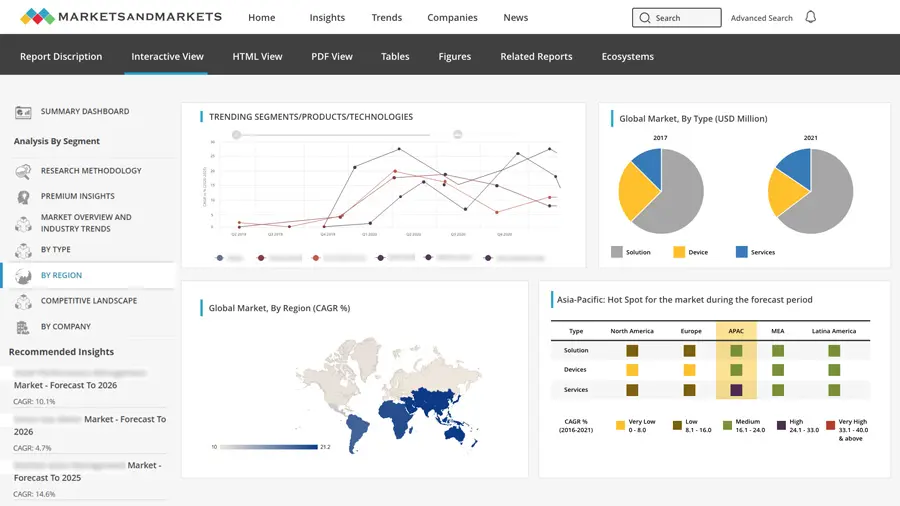
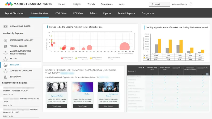
Growth opportunities and latent adjacency in AI Semiconductor Manufacturing Equipment Market