Photonic Packaging Market Size, Share, Trends & Growth by Packaging Technology (Flip-Chip Bonding, Wire Bonding, Wafer-Level Packaging), Optical Transceivers, Lasers & Light Sources, Data Centers and High-Performance Computing, Hyperscale Cloud Providers- Global Forecast to 2032


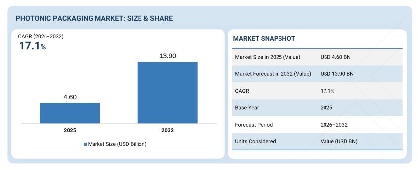
The global photonic packaging market was valued at USD 4.60 billion in 2025 and is projected to reach USD 13.90 billion by 2032, expanding at a compound annual growth rate (CAGR) of 17.1% during the 2026–2032 forecast period. This remarkable trajectory is being shaped overwhelmingly by one force: the insatiable bandwidth and power-efficiency demands of artificial intelligence infrastructure. As hyperscale operators race to deploy million-GPU clusters and next-generation AI training fabrics, conventional pluggable transceiver architectures are hitting physical limits, making photonic packaging — and particularly co-packaged optics — the critical enabling technology for the data center of the next decade.
Asia Pacific is the fastest-growing regional market, driven by aggressive AI data center buildouts in China, Japan, South Korea, and Singapore, indigenous silicon photonics initiatives, and state-backed semiconductor investment programs. North America holds the largest market base, underpinned by hyperscale cloud operator demand, CHIPS Act incentives, and a mature photonics ecosystem anchored by Intel, Broadcom, Cisco, and emerging CPO players such as Ayar Labs. Europe occupies a solid middle ground, with Germany and the UK leading demand through industrial photonics, coherent telecommunications, and EU-backed research programs in quantum and integrated photonics.
Top 10 Key Takeaways
- North America holds the largest regional base, driven by hyperscale cloud investment and the concentrated presence of silicon photonics leaders including Intel, Broadcom, and Cisco.
- Asia Pacific is the fastest-growing region, with China, Japan, South Korea, and Singapore accelerating domestic AI infrastructure and photonic semiconductor investment.
- Co-packaged optics (CPO) is the most disruptive packaging technology segment, transitioning from early-access trials in 2025 to volume deployments across hyperscale data centers.
- Silicon photonics is the dominant integration platform, enabling CMOS-compatible manufacturing and tight electrical-optical co-design within a single package.
- Data centers and high-performance computing represent the leading application vertical, capturing the majority of photonic packaging demand as AI workloads scale.
- The CHIPS and Science Act in the United States and equivalent European Chips Act initiatives are reshaping supply chains and incentivizing domestic photonic packaging capacity.
- Key players shaping market dynamics include Intel, Broadcom, Cisco, Coherent, Lumentum, TSMC, GlobalFoundries, Marvell Technology, Ayar Labs, and Fabrinet, among others.
- Thermal management and yield optimization in high-density photonic modules remain the near-term technical challenge most cited by systems integrators and hyperscale buyers.
- Supply chain concentration around III-V electro-absorption modulated laser (EML) components represents a material risk, with lead times extending well beyond 2026 for premium sources.
- Strategic implication: companies that secure foundry partnerships, advance chip-to-chip optical interconnect roadmaps, and invest in CPO qualification processes now will capture outsized share through 2032 and beyond.
Why Photonic Packaging Matters Now
Photonic packaging sits at the intersection of semiconductor packaging engineering, optical systems design, and high-speed communications — three domains that are simultaneously undergoing once-in-a-generation transitions. For decades, the packaging of photonic components remained a specialized, relatively niche discipline serving optical transceiver manufacturers for telecommunications and data center interconnects. That characterization is now obsolete. The rise of large-scale AI compute clusters, the global rollout of 5G networks, and the convergence of photonics with advanced CMOS manufacturing have catapulted photonic packaging to a strategic priority for the world's most influential semiconductor and cloud companies. [INTERNAL LINK: Silicon Photonics Market] [INTERNAL LINK: Co-Packaged Optics Market]
The macro context amplifies this urgency. Global data creation and consumption continue on an exponential path, with generative AI and foundation model training placing bandwidth demands on data center networks that copper electrical interconnects simply cannot meet at acceptable power envelopes. Every watt saved in optical interconnects translates directly to reduced cooling capital expenditure, lower operational energy costs, and expanded compute density — factors that determine competitiveness for hyperscale operators investing hundreds of billions of dollars in AI infrastructure over this decade. Photonic packaging is the engineering discipline that determines whether those interconnects can scale. [INTERNAL LINK: Data Center Optical Interconnects Market]
Simultaneously, regulatory and geopolitical forces are reshaping the photonic packaging supply chain. The US CHIPS and Science Act, the EU Chips Act, and equivalent programs in Japan, South Korea, and India are directing unprecedented public capital toward domestic semiconductor manufacturing — including silicon photonics foundries and advanced packaging facilities. Export controls on advanced semiconductor equipment and certain photonic components have created further incentives for supply chain diversification and regionalization. For strategy, procurement, and investment leaders, understanding the photonic packaging market is no longer optional — it is fundamental to technology roadmap planning in data infrastructure, telecommunications, and industrial sensing alike.
Photonic Packaging Market Trends
The single most consequential trend reshaping the photonic packaging market is the transition from pluggable optical transceivers to co-packaged optics architectures. Pluggable transceivers have been the workhorses of data center optical connectivity for over a decade, offering ease of replacement and standards-based interoperability. But the bandwidth demands of AI scale-out networks — where a single training cluster may require hundreds of terabits per second of internal connectivity — are pushing pluggable form factors toward their fundamental electrical limits. Co-packaged optics addresses this by moving the optical engine directly onto the package substrate alongside the switch ASIC or compute chip, drastically shortening the high-speed electrical trace and reducing power per bit by an estimated three to five times compared to equivalent pluggable solutions.
Silicon photonics is cementing itself as the integration platform of choice for high-volume photonic packaging. The technology's compatibility with mainstream CMOS manufacturing means that leading foundries including TSMC and GlobalFoundries can produce silicon photonic integrated circuits on the same process nodes used for digital logic — enabling cost structures and scaling trajectories that III-V-only platforms cannot match. TSMC's publicly stated position that silicon photonics is a 'More-than-Moore' pillar, and GlobalFoundries' acquisition of Singapore's Advanced Micro Foundry in late 2025, signal that silicon photonics is now a mainstream foundry offering rather than a specialty service.
Heterogeneous integration — combining silicon photonic dies with III-V laser chiplets, electronic driver ICs, and advanced packaging substrates within a single module — is the next technical frontier. Approaches including flip-chip bonding of InP lasers onto silicon waveguides, micro-transfer printing, and 3D stacking of electronic and photonic layers are all being actively developed by leading research groups and commercial players. The objective is to combine the cost and scalability advantages of silicon photonics with the superior light generation characteristics of III-V materials. Patent filings for silicon photonics packaging rose dramatically in 2024, with Broadcom, Intel, and TSMC leading the intellectual property arms race in this space.
AI-driven electronic design automation (EDA) is beginning to transform how photonic packages are designed. Traditional photonic circuit design has been a manual, expert-intensive process constrained by the complexity of simulating coupled optical, electrical, and thermal phenomena within a single package. Tools from Synopsys, Ansys Lumerical, and emerging startups are incorporating machine learning to accelerate design-space exploration, optimize coupling efficiency, and predict thermal failure modes before a single prototype is fabricated. This capability compression in design cycles is critical for reducing the time-to-market gap between photonic packaging innovations and the AI infrastructure they enable.
Photonic Packaging Market Drivers
The primary driver of photonic packaging market growth is the explosive, structurally unprecedented bandwidth demand emanating from AI and machine learning infrastructure. The shift from traditional cloud workloads — which can tolerate relatively modest interconnect latency — to AI training clusters, where thousands of accelerators must exchange gradient data continuously at extreme speeds, has fundamentally changed the economics of optical interconnect. Hyperscale operators such as Google, Meta, Microsoft, and Amazon are each spending tens of billions of dollars annually on data center construction, with a growing proportion of that capital earmarked for optical networking infrastructure. Each new generation of AI switch silicon — from 51.2T to 102.4T and beyond — demands corresponding advances in photonic packaging density and power efficiency.
The global rollout of 5G networks, and the earliest planning activity around 6G, is a second structural driver. Mobile fronthaul and backhaul architectures increasingly rely on coherent optical technology to carry the massive traffic volumes that 5G spectrum bands generate. Photonic packaging solutions that enable compact, high-reliability coherent modules are seeing sustained demand from telecom equipment manufacturers across all major geographies. As network operators prepare for the densification that 5G Advanced and eventual 6G will require, the specifications for optical transceivers and photonic integrated circuits will tighten further, sustaining demand for more sophisticated packaging approaches. [INTERNAL LINK: Coherent Optical Transceiver Market]
Energy efficiency regulation and corporate sustainability commitments are proving to be a surprisingly potent demand driver. Data centers currently consume approximately one to two percent of global electricity, a share that analysts widely expect to grow sharply as AI workloads scale. Regulatory pressure from the European Union's Energy Efficiency Directive and voluntary sustainability commitments from major hyperscalers are creating strong economic incentives to reduce power per bit in optical interconnects. Co-packaged optics, which eliminates the repeated electrical-to-optical and optical-to-electrical signal conversions inherent in pluggable architectures, is one of the few near-term technologies capable of delivering the step-change reductions in interconnect power that these sustainability goals demand.
Government industrial policy is an amplifying driver that deserves explicit recognition. The US CHIPS and Science Act has directed over USD 52 billion toward domestic semiconductor manufacturing and research, with silicon photonics and advanced packaging identified as strategic priorities. In Europe, the EU Chips Act targets a doubling of Europe's global semiconductor market share by 2030, with photonic integration identified as a key area of differentiation for European research institutes and fabless companies. Japan's NICT and industry consortia are advancing photonic integrated circuit standards. India's semiconductor mission is targeting advanced packaging capabilities. Collectively, these policy instruments are reshaping the geography of photonic packaging manufacturing and sustaining investment across the entire value chain.
Photonic Packaging Market Challenges and Restraints
The manufacturing complexity of advanced photonic packaging remains the market's most significant near-term restraint. Unlike digital semiconductor packaging — where automated pick-and-place and well-established assembly processes dominate — photonic packaging requires sub-micron optical alignment precision between laser sources, waveguides, photodetectors, and fiber interfaces. The coupling losses introduced by even nanometer-scale misalignment can render a module non-functional or degrade its performance below specification. Achieving this precision reliably at high volume and low cost is an engineering challenge that only a handful of contract manufacturers and vertically integrated players have solved at production scale. This manufacturing complexity translates directly into elevated costs and constrained capacity, particularly for the most advanced CPO and heterogeneous integration formats.
Supply chain concentration around III-V laser subcomponents represents a material systemic risk. Electro-absorption modulated lasers (EMLs), which are essential for high-speed optical modulation in silicon photonic modules, are produced by a small number of specialized manufacturers including Lumentum, Coherent, Mitsubishi Electric, and Sumitomo Electric. The surge in demand from AI infrastructure build-outs has created a structural supply bottleneck, with lead times for premium EML components extending well beyond anticipated delivery windows. This chokepoint is limiting the pace at which CPO and advanced transceiver volumes can ramp, and is driving hyperscale operators to pre-allocate foundry capacity years in advance — a dynamic that disadvantages smaller players and new market entrants.
The absence of fully standardized interfaces for co-packaged optics is a commercialization friction point. While industry bodies including the Optical Internetworking Forum (OIF), the IEEE, and multi-source agreement (MSA) groups are actively developing CPO interoperability standards, consensus is still forming. Without agreed standards for the electrical interface between the switch ASIC and the optical engine, or for the fiber connectivity at the module boundary, customers face interoperability uncertainty and increased qualification risk. This slows enterprise and telecommunications buyer adoption relative to the well-understood standards ecosystem surrounding pluggable transceiver form factors such as QSFP-DD and OSFP-XD.
Industry and Application Growth in the Photonic Packaging Market
Data centers and high-performance computing represent the dominant and fastest-scaling application vertical for photonic packaging. The architecture of modern AI training clusters — where thousands of GPU and custom AI accelerator chips must exchange activations and gradients across a high-bandwidth, low-latency fabric — is fundamentally dependent on optical interconnect performance. As cluster sizes scale from tens of thousands to hundreds of thousands of accelerators, the bandwidth demands placed on the photonic packaging ecosystem grow non-linearly. Broadcom's Tomahawk 6 co-packaged optics switch, NVIDIA's Spectrum-X and Quantum-X photonic switches announced in 2025, and Google's demonstrated deployments of optical circuit switching collectively illustrate the depth and urgency of data center demand for advanced photonic packaging solutions.
Telecommunications infrastructure is the second pillar of photonic packaging demand, with the 5G densification wave and the earliest 6G planning activities driving coherent optical module requirements at scale. Radio access network architectures that rely on centralized baseband processing require high-bandwidth fronthaul optical links between remote radio heads and centralized units — links that can only be served economically by photonically integrated coherent transceivers. In the long-haul and submarine cable segment, the unrelenting growth of internet backbone traffic is driving demand for higher-capacity coherent line cards with increasingly integrated photonic packaging. Nokia's acquisition of Infinera in 2024 and Cisco's build-out of its silicon photonics portfolio through the Acacia and Luxtera acquisitions reflect the strategic importance of photonic packaging capability in the telecom equipment market.
Healthcare and life sciences represent an emerging high-value application area for photonic packaging. Photonic integrated circuits are finding growing application in optical coherence tomography, flow cytometry, molecular diagnostics, and minimally invasive surgical guidance systems. The size, weight, and power advantages of integrated photonic packages compared to discrete bulk-optic assemblies are particularly compelling for handheld and point-of-care diagnostic devices. Several medical device original equipment manufacturers are actively qualifying photonic packaging solutions for FDA-regulated products, creating a demand stream that, while smaller in absolute terms than data centers or telecom, commands significantly higher average selling prices and offers attractive margin profiles for specialized packagers.
Automotive LiDAR is a fourth growth vertical, driven by the global deployment of advanced driver assistance systems and the long-term ambition for autonomous vehicle commercialization. Silicon photonics-based LiDAR architectures — which integrate the laser source, beam-steering elements, and photodetection arrays within a compact solid-state package — offer the cost, size, and reliability advantages needed for high-volume automotive applications. Fabless photonic IC designers such as Rockley Photonics, along with established automotive suppliers, are advancing LiDAR-specific photonic packaging designs. Defense and aerospace applications — encompassing free-space optical communications, directed energy systems, and inertial sensing — round out the application landscape with specialized, lower-volume but high-specification demand. [INTERNAL LINK: LiDAR Market] [INTERNAL LINK: Automotive Sensing Market]
Photonic Packaging Market Segment Insights
By Packaging Technology
Co-packaged optics is the most strategically important packaging technology format, though it is still in the early stages of volume commercialization as of 2025. Flip-chip bonding currently dominates deployed volumes, serving as the workhorse assembly technique for silicon photonic transceivers and module-level integration across data center and telecom applications. The precision alignment capabilities and robust electrical interconnect density of flip-chip processes make it the default choice for mainstream production.
Co-packaged optics is unambiguously the fastest-growing technology segment, transitioning from engineering samples and early-access programs in 2025 toward broader hyperscale deployments anticipated through 2026 and 2027. The power efficiency and bandwidth density advantages of CPO — which integrates the optical engine directly on the package substrate of the switch ASIC — are compelling enough that every major hyperscale operator and switch silicon vendor has CPO programs underway. Wafer-level packaging and 3D heterogeneous integration formats are also growing rapidly as process maturity improves.
By Component
Optical transceivers are the largest component segment by revenue, reflecting their ubiquity as the optical connectivity building block in both data center and telecom deployments. The rapid cadence of transceiver generation upgrades — from 400G to 800G and now into 1.6T configurations — is sustaining high average selling prices and component volumes simultaneously. Lasers and light sources represent the second-largest component category, with their performance characteristics — output power, linewidth, modulation bandwidth, and reliability — serving as primary determinants of overall module performance.
Modulators are the fastest-growing component segment, propelled by the emergence of co-packaged optics architectures that require ultra-high-speed optical modulators integrated within a tight footprint. Micro-ring modulators and Mach-Zehnder modulator arrays operating at 100G and 200G per lane are enabling the bandwidth density of next-generation CPO products. The development of 400 mW continuous-wave lasers optimized for silicon photonics and CPO applications by Coherent in late 2025 illustrates the pace of component advancement supporting this growth.
By Application
Data centers and high-performance computing lead all application segments by both revenue and growth rate trajectory, reflecting the AI infrastructure buildout that is reshaping global capital expenditure patterns. The specific dynamics within data center photonic packaging — increasing port speeds, growing CPO adoption, and the shift toward custom AI switch silicon from hyperscalers — create a demand environment that is both large in absolute terms and structurally accelerating rather than maturing.
Telecommunications is the second-largest application, with coherent optical technologies for long-haul, metro, and mobile fronthaul applications sustaining steady demand for high-performance photonic packaging. Healthcare and life sciences is the fastest-growing non-data-center application vertical, driven by regulatory approval of photonic-enabled diagnostic devices and the expansion of photonic sensing into consumer health monitoring applications.
By Material
Silicon-based substrates lead the photonic packaging materials segment, a direct consequence of silicon photonics' dominance as the integration platform for high-volume optical transceiver and CPO production. The CMOS process compatibility of silicon substrates enables cost structures and manufacturing scalability that no competing material platform can match at the volumes required for data center applications.
III-V compound semiconductor materials, particularly indium phosphide and gallium arsenide, are the fastest-growing specialty materials segment. As heterogeneous integration techniques for bonding III-V laser chiplets onto silicon photonic platforms mature, demand for high-quality III-V wafers and epitaxial structures is growing in direct proportion to the CPO adoption curve. Lithium niobate on insulator is an emerging material platform gaining attention for its exceptional electro-optic modulation efficiency, with potential application in ultra-high-speed modulators.
By End User
Hyperscale cloud providers — including the major US operators and their counterparts in China, including Alibaba Cloud, Tencent Cloud, ByteDance, and Baidu — are the dominant end-user category by volume and the primary catalyst for photonic packaging technology evolution. Their requirements for customized, high-reliability optical components at unprecedented scale are setting the technical agenda for the entire supply chain, from foundry process development to packaging automation.
Semiconductor and photonic IC manufacturers are the fastest-growing end-user segment as silicon photonics capabilities move from research and early production into high-volume manufacturing across an expanding ecosystem of fabless designers and foundry customers. The emergence of fabless photonic IC companies — including Ayar Labs, Celestial AI, and Lightmatter — accessing silicon photonics foundry services from TSMC, GlobalFoundries, and others is creating a new category of end-user demand that did not exist at scale five years ago.
Key Segmentation Conclusions
- Co-packaged optics is the highest-growth packaging technology format, with deployment velocity accelerating as hyperscale CPO programs mature from early access to production.
- Optical transceivers dominate current component revenue, while modulators and laser sources are the fastest-evolving sub-segments driven by CPO and heterogeneous integration requirements.
- Data centers and HPC capture the largest application share, with healthcare photonics emerging as the premium-priced growth opportunity for specialized packagers.
- Silicon photonics dominates material platforms; III-V heterogeneous integration and lithium niobate are the next frontier materials gaining commercial traction.
- Hyperscale cloud providers set the technical and commercial agenda; fabless photonic IC designers are the fastest-growing end-user category entering the supply chain.
Photonic Packaging Market — Regional Analysis
North America
North America remains the largest regional market for photonic packaging, driven by the extraordinary concentration of hyperscale cloud infrastructure investment, a deep technology ecosystem spanning semiconductor design, photonic component manufacturing, and systems integration, and robust government support through the CHIPS and Science Act. The United States is home to the most significant demand engines in the global photonic packaging market — the hyperscale data center operators investing at a pace that is restructuring global optical component supply chains. Valued at USD 1.72 billion in 2025 and projected to reach USD 5.21 billion by 2032 at a CAGR of 17.2%, the North American photonic packaging market combines scale with sustained growth momentum. US policy interventions, including CHIPS Act grants for silicon photonics manufacturing and export controls that are driving domestic supply chain investment, are reinforcing the region's competitive position. Canada is emerging as a secondary hub, with government-backed photonics R&D centers and new collaborative programs with UK institutions developing co-packaged optical engines for AI data center applications. Mexico's role is primarily in advanced packaging assembly, where cost advantages and proximity to US hyperscale facilities are attracting investment.
Europe
Europe's photonic packaging market is characterized by strong industrial photonics demand, a coherent regulatory framework through the EU Chips Act, and world-class research institutions that are advancing the technology frontier in silicon photonics, quantum photonics, and heterogeneous integration. Valued at USD 1.04 billion in 2025 and forecast to reach USD 2.86 billion by 2032 at a CAGR of 15.6%, Europe's market grows at a somewhat more moderate pace than Asia Pacific or North America, reflecting the region's relatively smaller hyperscale cloud infrastructure footprint compared to its US and Asian counterparts. Germany leads European demand, anchored by strong industrial laser and photonic sensing markets in automotive, precision manufacturing, and medical technology. The United Kingdom hosts a vibrant photonic integration research community, with institutions including the University of Southampton and the Compound Semiconductor Applications Catapult playing internationally significant roles. France, the Netherlands, and the Nordic countries contribute significant demand from telecom infrastructure upgrades and government-backed semiconductor research programs. The EU's emphasis on technological sovereignty and its support for the imec research consortium in Belgium are sustaining European competitive positioning in photonic packaging process development.
Asia Pacific
Asia Pacific is the fastest-growing regional market for photonic packaging, propelled by the most aggressive AI data center buildout programs in the world, state-backed semiconductor investment strategies, and the presence of leading foundries and contract manufacturers in the supply chain. Valued at USD 1.31 billion in 2025 and projected to surge to USD 4.42 billion by 2032 at a CAGR of 19.0%, the region's growth trajectory reflects both scale-up of existing capacity and the development of entirely new domestic photonic packaging ecosystems. China's domestic AI ambitions — pursued by Alibaba Cloud, Tencent Cloud, ByteDance, and Baidu — are catalyzing a parallel CPO development ecosystem even as export controls constrain access to certain advanced foreign GPU types, incentivizing indigenous silicon photonics and packaging innovation. Japan's NTT Innovative Photonics and Industry Consortium, NICT research programs, and TSMC's joint venture semiconductor facility in Kumamoto reflect the country's strategic commitment to photonic integration leadership. South Korea's Samsung and SK Hynix are expanding into advanced photonic packaging adjacent to their memory and advanced logic packaging capabilities. Singapore has positioned itself as a premier Asia Pacific hub for photonic component assembly and test, while India's semiconductor mission is beginning to target advanced packaging capabilities that could serve the photonic packaging value chain in the years ahead.
Rest of World
The Rest of World segment, encompassing Latin America, the Middle East, and Africa, represents the smallest regional base but offers meaningful emerging demand pockets tied to infrastructure modernization and sovereign digital economy ambitions. Valued at USD 0.53 billion in 2025 and projected to reach USD 1.41 billion by 2032 at a CAGR of 15.0%, the region's growth is concentrated in the Gulf Cooperation Council states and Brazil. Saudi Arabia's NEOM mega-project and Vision 2030 digital infrastructure programs are driving data center construction at unprecedented pace, creating demand for advanced optical interconnect solutions including photonic packaging products. The UAE, particularly through Abu Dhabi's AI hub ecosystem and Dubai's continued data center expansion, represents the Middle East's most active photonic packaging demand market. Brazil anchors Latin American demand through its large enterprise and telecom operator base, government-backed broadband expansion programs, and growing interest in domestically-assembled optical networking equipment. South Africa, while a smaller market, serves as a gateway to Sub-Saharan African data center growth driven by hyperscale entry from Microsoft Azure and Amazon Web Services.
Regional Outlook Summary
- North America leads in absolute market size, sustained by hyperscale AI infrastructure investment and a policy environment actively supporting domestic silicon photonics manufacturing.
- Asia Pacific delivers the highest regional CAGR, with China, Japan, and South Korea each running independent photonic packaging development programs of strategic national significance.
- Europe's growth is moderate but structurally sound, anchored in industrial photonics, coherent telecom, and EU-funded research programs advancing next-generation integration platforms.
- The Middle East — led by Saudi Arabia and the UAE — is the fastest-growing sub-region within Rest of World, converting sovereign wealth into data center and AI infrastructure investment at an accelerating pace.
- Regional supply chain diversification, driven by geopolitical pressure and industrial policy, is creating new photonic packaging manufacturing hubs beyond the traditional East Asia concentration — including Europe and North America.
Country-Specific Insights in the Photonic Packaging Market
The United States is the single most important national market for photonic packaging globally, combining the world's largest concentration of hyperscale cloud operators, the deepest venture and corporate R&D investment in silicon photonics, and an increasingly activist industrial policy posture. The CHIPS and Science Act is directing investment toward domestic silicon photonics foundry capacity — a gap that GlobalFoundries, Intel Foundry Services, and Tower Semiconductor are each working to fill. Export control regimes are simultaneously constraining certain cross-border technology transfers, creating both risk (supply chain disruption) and opportunity (onshoring incentives) for US-based photonic packaging players.
China represents a unique strategic case — simultaneously a massive demand market and a geography where supply chain access is increasingly constrained by geopolitical dynamics. Domestic hyperscalers are aggressively qualifying indigenous CPO and silicon photonics solutions, creating demand for Chinese fabless photonic IC designers and domestic packaging houses. State-backed investment in compound semiconductor manufacturing, epitaxial growth capabilities, and advanced packaging processes is accelerating, though the technology gap relative to leading global players in silicon photonics remains significant.
Japan occupies a distinctive role as both a strategic research and manufacturing hub. The Photonics Electronics Technology Research Association (PETRA), NTT's investments in photonic-electronic convergence, and the TSMC Kumamoto facility collectively position Japan as a leading site for advanced photonic packaging process development. Japan's strength in precision assembly equipment and materials — including optical adhesives, high-purity substrates, and specialty coatings — gives it a complementary role in the global photonic packaging value chain beyond chip fabrication alone.
Germany commands the European industrial photonics market, with the country's laser manufacturing cluster in Bavaria and Baden-Wuerttemberg producing a significant share of global fiber laser and industrial photonics output. German automotive OEMs and their Tier 1 suppliers are among the most active evaluators of photonic LiDAR packaging solutions, providing a domestic demand anchor that complements the country's manufacturing strengths. The United Kingdom's photonic integration research community, commercialized through the Compound Semiconductor Applications Catapult and university spinouts, is generating a pipeline of specialized photonic packaging technologies including low-loss fiber coupling solutions and quantum photonic packages.
Country-Level Conclusions
- The United States is the dominant single-country market, shaping global CPO and silicon photonics packaging standards through hyperscale operator demand and CHIPS Act-driven manufacturing investment.
- China is pursuing photonic packaging self-sufficiency aggressively, with state-backed programs compensating partially for constrained access to leading-edge foreign technology.
- Japan's combination of precision manufacturing heritage, NTT research programs, and new advanced foundry capacity positions it as a critical node in the Asia Pacific photonic packaging supply chain.
- Germany leads European demand through its industrial photonics and automotive sectors; the UK contributes research-driven innovation and compound semiconductor packaging expertise.
- The Gulf states — particularly Saudi Arabia and the UAE — are the most dynamic emerging national markets, converting sovereign AI infrastructure investment into photonic packaging demand at an accelerating rate.
Key Company Insights in the Photonic Packaging Market
The photonic packaging competitive landscape features a diverse ecosystem spanning vertically integrated giants, specialty photonic component manufacturers, pure-play silicon photonics foundries, advanced packaging contract manufacturers, and a growing cohort of well-funded fabless photonic IC startups. The key players shaping market dynamics include:
- Intel Corporation
- Broadcom Inc.
- Cisco Systems, Inc.
- Coherent Corp.
- Lumentum Holdings, Inc.
- TSMC (Taiwan Semiconductor Manufacturing Company)
- GlobalFoundries Inc.
- Marvell Technology, Inc.
- Fabrinet
- Ayar Labs Inc.
- STMicroelectronics N.V.
- IBM Corporation
- Ranovus Inc.
- NVIDIA Corporation
- Sumitomo Electric Industries, Ltd.
Intel continues to evolve its silicon photonics strategy, reporting strong year-over-year revenue growth in its optical business in 2024 driven by shipments into large AI GPU cluster environments. The company's silicon photonics platform, which combines an optical transceiver architecture with its foundry capabilities, provides a differentiated position in the CPO transition. Broadcom is advancing its co-packaged optics roadmap with the third-generation Tomahawk 6 (TH6-Davisson) CPO switch, developed in collaboration with TSMC, HPE, and Micas Networks, and is shipping to early-access hyperscale customers. Cisco, whose silicon photonics capabilities were significantly strengthened through the Acacia and Luxtera acquisitions, demonstrated its 1.6T optical transceiver lineup and AI networking solutions at OFC 2026, consolidating its position as the leading networking equipment provider for AI data center deployments.
Coherent unveiled 400 mW continuous-wave lasers specifically designed for silicon photonics and CPO applications in September 2025 — a critical component enabling higher-power CPO modules with improved power budgets. Lumentum, as the only supplier currently shipping 200G-per-lane EMLs at production volumes, holds a strategic chokepoint position in the CPO supply chain. NVIDIA invested in both Lumentum and Coherent through supply agreements in April 2026, seeking to secure laser component capacity for its silicon photonics switch roadmap. TSMC's COUPE advanced packaging platform provides the substrate integration infrastructure for NVIDIA's CPO switches, cementing the foundry's role as the backbone of the most advanced photonic packaging programs. GlobalFoundries' acquisition of Advanced Micro Foundry in late 2025 expanded its silicon photonics capacity significantly, offering a China-free supply chain option that US hyperscalers increasingly value. Ayar Labs has integrated its optical engines into GUC's advanced packaging workflow, advancing the commercialization pathway for chiplet-based CPO architectures that could ultimately deliver optical I/O directly at the processor package level.
Key Company Strategy Conclusions
- Vertical integration and supply security are defining strategic priorities: NVIDIA's investments in Lumentum and Coherent, Cisco's Acacia acquisition, and GlobalFoundries' AMF acquisition all reflect the premium placed on controlling critical photonic supply chain nodes.
- Co-packaged optics program execution speed is becoming the primary competitive differentiator among switch silicon vendors and photonic module manufacturers.
- Foundry capacity at TSMC, GlobalFoundries, and Intel Foundry Services is the gating constraint for CPO volume ramp — companies securing wafer commitments early hold structural advantages.
- Fabless photonic IC startups including Ayar Labs, Celestial AI, and Lightmatter are pursuing chiplet-based optical I/O strategies that, if successful, could disrupt established transceiver and CPO architectures.
- AI-driven EDA tools from Synopsys and Ansys Lumerical are compressing photonic package design cycles, enabling faster iteration and reducing development costs for both incumbents and new entrants.
Recent Developments in the Photonic Packaging Market
- In April 2026, NVIDIA invested USD 4 billion in supply agreements with Lumentum and Coherent, securing laser component capacity for its silicon photonics switch roadmap as AI cluster bandwidth demands intensify.
- In April 2026, Broadcom expanded its co-packaged optics roadmap partnerships with hyperscale cloud providers, focusing on next-generation switch silicon integration with the TH6-Davisson CPO switch designed for AI data center networking at 102.4 Tbps.
- In March 2026, Cisco Systems unveiled its 1.6T optical transceivers, 800G linear pluggables, and AI networking solutions at OFC 2026 in Los Angeles, built on its silicon photonics platform.
- In November 2025, GlobalFoundries completed its acquisition of Advanced Micro Foundry (AMF) in Singapore, establishing itself as the largest dedicated silicon photonics foundry outside China and offering a geopolitically diversified fabrication option for hyperscale customers.
- In May 2025, AMD acquired Enosemi, a photonic integrated circuit design firm, to accelerate its development of co-packaged optics for AI systems and strengthen its position in energy-efficient optical interconnect for chip-to-chip communication.
Real-World Use Cases and Case Studies
NVIDIA's Quantum-X and Spectrum-X Photonic Switch Deployments (2025–2026): In March 2025, NVIDIA announced the Spectrum-X and Quantum-X photonic switch families, developed in partnership with TSMC using co-packaged silicon photonics technology. The Quantum-X switch, entering availability in the second half of 2025, delivers 115.2 terabits per second of total throughput by integrating six silicon photonic engines per CPO module alongside a 107-billion-transistor ASIC built on TSMC's 4N process. The motivation was direct: as NVIDIA's customers began deploying GPU clusters exceeding 10,000 accelerators per data hall, the electrical I/O bandwidth and power consumption of conventional pluggable transceivers became an architectural bottleneck. The CPO architecture achieves approximately a 3.5x reduction in interconnect power per bit, enabling denser compute configurations within the thermal and power envelope of next-generation AI facilities.
AMD's Enosemi Acquisition for AI Optical Interconnects (2025): In May 2025, AMD acquired Enosemi, a startup specializing in photonic integrated circuit design for co-packaged optics applications. The strategic objective was to develop chip-to-chip optical interconnect solutions that could ultimately reduce the latency and power consumption of connections between AI accelerators at the package or board level — a capability that would complement AMD's Instinct GPU and EPYC processor roadmaps. By bringing photonic IC design expertise in-house, AMD signaled its intention to compete with NVIDIA and Intel across the full optical interconnect stack, not merely at the chip compute layer, reflecting the degree to which photonic packaging has become a first-order strategic asset in the AI semiconductor industry.
Photonic Packaging Market Segmentation
The photonic packaging market is segmented across five primary dimensions: packaging technology, component type, application vertical, material platform, and end user. By packaging technology, the market spans flip-chip bonding — the current volume leader — through wire bonding, wafer-level packaging, co-packaged optics, and emerging 3D heterogeneous integration formats. The transition toward CPO represents the dominant directional force shaping technology mix evolution through the forecast period, as hyperscale operator demand drives adoption of packaging architectures that could not have been cost-effectively manufactured even three years ago.
Component segmentation reveals the breadth of the photonic packaging value chain, from optical transceivers and laser sources to photodetectors, waveguides, high-speed modulators, and wavelength multiplexing elements. Each component category has distinct performance-cost tradeoffs and technology development timescales. The data center application dominates the application segmentation hierarchy, followed by telecommunications and the emerging healthcare, automotive, defense, and industrial verticals. Material segmentation captures the silicon photonics-to-III-V-to-polymer spectrum, with silicon commanding dominant share and III-V heterogeneous integration growing as CPO architecture requires bonded laser chiplets on silicon waveguide platforms. End-user segmentation distinguishes hyperscale cloud operators from telecom equipment manufacturers, semiconductor foundries, medical device OEMs, automotive OEMs, and government defense agencies — each with distinct qualification standards, buying cycles, and performance specifications.
Market Segmentation Summary
- The packaging technology segmentation is experiencing the most rapid structural shift of any axis, as CPO transitions from early-access programs toward production-scale deployments in hyperscale data centers.
- Application segmentation is heavily weighted toward data centers and HPC, but the fastest-growing adjacent verticals — healthcare, automotive LiDAR, and defense — are opening high-value specialty market pockets.
- Component segmentation growth is uneven: transceivers provide the revenue base while modulators and laser chiplets are the fastest-evolving growth vectors.
- Material platform segmentation is bifurcating between high-volume silicon photonics and high-performance III-V platforms — with heterogeneous integration techniques increasingly bridging the two.
- End-user segmentation is shifting as fabless photonic IC designers emerge as a distinct, fast-growing demand category accessing foundry services rather than purchasing vertically integrated products.
Conclusion and Future Outlook
The photonic packaging market is entering a decade of structural transformation rather than incremental evolution. The forces driving this transformation — AI infrastructure scale-out, 5G/6G network densification, energy efficiency imperatives, and national industrial policy — are compounding rather than competing. Each new generation of AI accelerator demands better optical interconnect, which demands better photonic packaging, which demands more advanced foundry processes, which attracts more capital investment, which enables the next generation of AI accelerators. This virtuous cycle is self-reinforcing in a way that conventional semiconductor market dynamics rarely are, and it is why the photonic packaging market is expected to nearly triple in value between 2025 and 2032 while simultaneously advancing technically at a pace that will make today's state-of-the-art products look conservative within a few years.
Artificial intelligence will not merely be a demand driver for photonic packaging — it will actively reshape how photonic packages are designed, manufactured, and tested. AI-driven EDA tools are already compressing design cycles. Machine learning-based process control is beginning to improve yield in high-volume photonic assembly. Digital twin models of thermal and optical behavior within complex packages are reducing prototype iteration counts. As these capabilities mature through the forecast period, the barrier to photonic packaging innovation will shift from design expertise — which AI tools are democratizing — toward manufacturing process mastery and foundry relationships, which will remain the true sources of competitive advantage for the market's leading players. For businesses considering their positioning in this market, the strategic calculus is clear: secure supply chain relationships early, invest in CPO qualification before volume demand fully materializes, and treat photonic packaging capability not as a commodity procurement category but as a core technology asset that will determine competitive positioning in AI infrastructure, telecommunications, and advanced sensing for the remainder of this decade.
Frequently Asked Questions (FAQ) Photonic Packaging Market
1. How big is the photonic packaging market?
The global photonic packaging market was valued at USD 4.60 billion in 2025 and is projected to reach USD 13.90 billion by 2032. This growth reflects sustained demand from AI data center infrastructure, 5G/6G telecommunications, and expanding applications in healthcare and automotive sensing. North America currently holds the largest regional market share, while Asia Pacific is the fastest-growing region.
2. What is the photonic packaging market growth rate?
The photonic packaging market is expected to grow at a CAGR of 17.1% from 2026 to 2032. This growth rate is driven by the extraordinary bandwidth demands of AI training clusters, the transition from pluggable transceivers to co-packaged optics architectures, and government industrial policy programs in the US, Europe, and Asia Pacific that are sustaining investment across the photonic packaging value chain.
3. Which segment leads the photonic packaging market?
By application, data centers and high-performance computing represent the leading segment, driven by hyperscale cloud operator demand for high-speed, energy-efficient optical interconnects in AI infrastructure. By packaging technology, flip-chip bonding currently leads in deployed volumes, though co-packaged optics is the fastest-growing format and is expected to capture a progressively larger share of the market through the forecast period. Silicon photonics is the dominant integration platform across segments.
4. Who are the key players in the photonic packaging market?
The leading companies in the photonic packaging market include Intel Corporation, Broadcom Inc., Cisco Systems, Coherent Corp., Lumentum Holdings, TSMC, GlobalFoundries, Marvell Technology, Fabrinet, and Ayar Labs, among others. The competitive landscape also features IBM, STMicroelectronics, Ranovus, NVIDIA, and Sumitomo Electric Industries. The market is characterized by intense strategic activity including acquisitions, supply agreements, foundry partnerships, and co-development programs across the value chain.
5. What are the key factors driving the photonic packaging market?
The primary drivers of the photonic packaging market are: the explosive bandwidth and power-efficiency demands of AI training clusters and hyperscale data centers; the 5G/6G rollout creating sustained demand for coherent optical transceivers; energy efficiency imperatives and corporate sustainability commitments accelerating co-packaged optics adoption; and government industrial policy programs including the US CHIPS Act and EU Chips Act directing capital toward domestic silicon photonics and advanced packaging manufacturing. Collectively, these drivers are structurally reinforcing rather than cyclical, supporting the market's sustained double-digit CAGR through 2032.
Speak with a MarketsandMarkets Analyst
The photonic packaging market is evolving rapidly across technology, geography, and competitive dimensions that standard market intelligence cannot fully capture. MarketsandMarkets provides deep, segment-level intelligence — including granular sub-segment forecasts, company capability benchmarking, supply chain risk analysis, and CPO adoption timelines by hyperscale operator — that enables strategy, procurement, and investment leaders to make decisions with confidence. To request a sample of the full report, customize the scope to your specific technology or geographic focus, or speak directly with our photonics and semiconductor packaging analyst team, contact us through our website. Insight that moves with the market, delivered to your strategic timeline.
 Exclusive indicates content/data unique to MarketsandMarkets and not available with any competitors.
TABLE OF CONTENTS
1 Introduction
1.1 Study Objectives
1.2 Market Definition and Scope
1.3 Inclusions and Exclusions
1.4 Study Scope
1.4.1 Markets Covered
1.4.2 Geographic Segmentation
1.4.3 Years Considered
1.5 Currency Considered
1.6 Stakeholders
2 Research Methodology
2.1 Research Approach
2.2 Secondary Research
2.3 Primary Research
2.3.1 Primary Interviews and Key Industry Experts
2.3.2 Key Primary Research Insights
2.3.3 Breakdown of Primaries
2.4 Market Size Estimation
2.4.1 Bottom-Up Approach
2.4.2 Top-Down Approach
2.5 Data Triangulation
2.6 Assumptions and Limitations
3 Executive Summary
4 Premium Insights
4.1 Attractive Opportunities in the Photonic Packaging Market
4.2 Photonic Packaging Market, by Packaging Technology
4.3 Photonic Packaging Market, by Application
4.4 Photonic Packaging Market, by Region
5 Market Overview
5.1 Introduction
5.2 Market Dynamics
5.2.1 Drivers
5.2.1.1 Explosive Bandwidth Demand from AI and Hyperscale Data Centers
5.2.1.2 5G/6G Rollout Driving Next-Generation Optical Interconnects
5.2.1.3 Energy Efficiency Imperatives Accelerating Co-Packaged Optics Adoption
5.2.2 Restraints
5.2.2.1 High Manufacturing Complexity and Cost of Advanced Photonic Packaging
5.2.2.2 Shortage of Specialized Talent and Process Expertise
5.2.3 Opportunities
5.2.3.1 Emergence of Co-Packaged Optics as a Disruptive Packaging Paradigm
5.2.3.2 Healthcare and LiDAR Applications Opening Adjacent Markets
5.2.4 Challenges
5.2.4.1 Thermal Management and Reliability in High-Density Modules
5.2.4.2 Supply Chain Concentration Risk for III-V Laser Subcomponents
5.3 Value Chain Analysis
5.4 Ecosystem Analysis
5.5 Investment and Funding Scenario
5.6 Pricing Analysis
5.7 Trends and Disruptions Impacting Customer Business
5.8 Technology Analysis
5.8.1 Key Technologies: Silicon Photonics, Co-Packaged Optics, Heterogeneous Integration
5.8.2 Complementary Technologies: Advanced Semiconductor Packaging, CMOS Integration
5.8.3 Adjacent Technologies: Quantum Photonics, Free-Space Optics
5.9 Porter's Five Forces Analysis
5.10 Key Stakeholders and Buying Criteria
5.11 Case Study Analysis
5.12 Trade Analysis
5.13 Patent Analysis
5.14 Key Conferences and Events
5.15 Regulatory Landscape
5.16 Impact of AI and Generative AI on the Photonic Packaging Market
5.17 Impact of 2025 US Tariffs on the Photonic Packaging Market
6 Industry Trends
6.1 Transition from Pluggable Transceivers to Co-Packaged Optics
6.2 Silicon Photonics as the Dominant Integration Platform
6.3 III-V Laser Hybrid Integration Advancements
6.4 Wafer-Level and Panel-Level Packaging Scaling
6.5 AI-Driven EDA and Design Automation for Photonic Packages
6.6 Sustainability and Power-per-Bit Optimization
7 Strategic Disruption and Technology Adoption Landscape
7.1 Co-Packaged Optics — Technology Readiness and Commercialization Timeline
7.2 Heterogeneous Integration Roadmaps (2.5D, 3D-IC, Chiplets)
7.3 Impact of CHIPS and Science Act and National Semiconductor Strategies
7.4 Geopolitical Fragmentation and Supply Chain Re-Shoring
7.5 Standards Development (IEEE, OIF, MSA) Impacting Interoperability
8 Customer Landscape and Buyer Behavior
8.1 Decision-Making Process and Procurement Cycles
8.2 Key Buyer Stakeholder Groups
8.3 Adoption Barriers and Evaluation Criteria
8.4 Customer Segmentation by End-Use Profile
9 Photonic Packaging Market, by Packaging Technology
9.1 Introduction
9.2 Flip-Chip Bonding
9.3 Wire Bonding
9.4 Wafer-Level Packaging (WLP)
9.5 Co-Packaged Optics (CPO)
9.6 3D Heterogeneous Integration
9.7 Others (Micro-Transfer Printing, Panel-Level Packaging)
10 Photonic Packaging Market, by Component
10.1 Introduction
10.2 Optical Transceivers
10.3 Lasers and Light Sources
10.4 Photodetectors
10.5 Waveguides and Optical Fibers
10.6 Modulators
10.7 Multiplexers and Demultiplexers
10.8 Others (Attenuators, Switches, Isolators)
11 Photonic Packaging Market, by Application
11.1 Introduction
11.2 Data Centers and High-Performance Computing
11.3 Telecommunications (5G/6G Infrastructure)
11.4 Healthcare and Life Sciences (Medical Imaging, Diagnostics)
11.5 Automotive and LiDAR
11.6 Consumer Electronics
11.7 Defense and Aerospace
11.8 Industrial Manufacturing
12 Photonic Packaging Market, by Material
12.1 Introduction
12.2 Silicon-Based Substrates
12.3 III-V Compound Semiconductors (InP, GaAs)
12.4 Polymer Waveguide Materials
12.5 Glass and Silica Substrates
12.6 Others (Lithium Niobate, Diamond)
13 Photonic Packaging Market, by End User
13.1 Introduction
13.2 IT and Telecommunications Enterprises
13.3 Hyperscale Cloud Providers
13.4 Semiconductor and Photonic IC Manufacturers
13.5 Healthcare Institutions and Medical Device OEMs
13.6 Automotive OEMs and Tier 1 Suppliers
13.7 Defense and Government Agencies
14 Photonic Packaging Market, by Region
14.1 Introduction
14.2 North America
14.2.1 United States
14.2.2 Canada
14.2.3 Mexico
14.3 Europe
14.3.1 Germany
14.3.2 United Kingdom
14.3.3 France
14.3.4 Italy
14.3.5 Spain
14.3.6 Rest of Europe
14.4 Asia Pacific
14.4.1 China
14.4.2 Japan
14.4.3 South Korea
14.4.4 India
14.4.5 Singapore
14.4.6 Australia
14.4.7 Rest of Asia Pacific
14.5 Rest of World
14.5.1 Brazil
14.5.2 UAE
14.5.3 Saudi Arabia
14.5.4 South Africa
14.5.5 Rest of Rest of World
15 Competitive Landscape
15.1 Overview
15.2 Key Player Strategies and Right to Win
15.3 Revenue Analysis
15.4 Market Share Analysis
15.5 Company Evaluation Matrix — Key Players
15.5.1 Stars
15.5.2 Emerging Leaders
15.5.3 Pervasive Players
15.5.4 Participants
15.6 Company Evaluation Matrix — Startups and SMEs
15.6.1 Progressive Companies
15.6.2 Responsive Companies
15.6.3 Dynamic Companies
15.6.4 Starting Blocks
15.7 Competitive Benchmarking
15.8 Competitive Scenario
15.8.1 Product Launches (2024–2026)
15.8.2 Deals, Partnerships, Acquisitions, and Expansions (2024–2026)
16 Company Profiles
16.1 Intel Corporation
16.2 Broadcom Inc.
16.3 Cisco Systems, Inc.
16.4 Coherent Corp.
16.5 Lumentum Holdings, Inc.
16.6 TSMC (Taiwan Semiconductor Manufacturing Company)
16.7 GlobalFoundries Inc.
16.8 Marvell Technology, Inc.
16.9 Fabrinet
16.10 Ayar Labs Inc.
16.11 STMicroelectronics N.V.
16.12 IBM Corporation
16.13 Ranovus Inc.
16.14 NVIDIA Corporation
16.15 Sumitomo Electric Industries, Ltd.
17 Appendix
17.1 Discussion Guide
17.2 KnowledgeStore — Subscription Portal
17.3 Customization Options
17.4 Related Reports
17.5 Author Details











Growth opportunities and latent adjacency in Photonic Packaging Market