Semiconductor Grade Encapsulants Market Size, Share & Growth Report by Material Type (Epoxy-Based Encapsulants, Silicone-Based Encapsulants), Epoxy Resin, Silicone, MEMS & Sensors, Wire Bonding and Flip Chip Packaging, Consumer Electronics, Automotive - Global Forecast to 2032


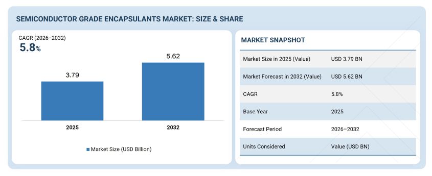
The global semiconductor grade encapsulants market was valued at approximately USD 3.79 billion in 2025 and is projected to reach USD 5.62 billion by 2032, registering a compound annual growth rate (CAGR) of approximately 5.8% during the forecast period 2026 to 2032. This growth is being driven primarily by the explosive proliferation of advanced semiconductor packaging technologies — including 2.5D and 3D integration, fan-out wafer-level packaging, and system-in-package architectures — that are, in turn, accelerating demand for high-performance encapsulants capable of protecting increasingly complex and thermally stressed die configurations in AI, high-performance computing, automotive, and 5G applications.
Asia Pacific is the fastest-growing region, propelled by the dense concentration of semiconductor OSATs and foundries across Taiwan, South Korea, China, and Japan, combined with rapidly expanding demand from domestic automotive and consumer electronics manufacturers. North America holds the largest share among Western geographies, driven by AI accelerator fab investments, CHIPS Act-funded capacity expansion, and the anchoring presence of leading fabless chip companies whose packaging partners consume semiconductor grade encapsulants at scale.
Top 10 Key Takeaways
- Asia Pacific is the dominant and fastest-growing regional market, anchored by Taiwan, South Korea, China, and Japan's dense OSAT and foundry ecosystems
- North America is the largest Western market, supported by CHIPS Act-driven fab investments and the data-center AI accelerator boom
- Epoxy-based encapsulants — particularly epoxy molding compounds — lead across all major application segments due to their cost-performance balance and process maturity
- Silicone-based encapsulants are the fastest-growing material type, gaining share in automotive electronics and harsh-environment applications
- The automotive application segment is the fastest-growing end-use vertical, propelled by ADAS proliferation and the electrification of powertrains
- The data center and high-performance computing segment is emerging as a structurally significant demand driver, as AI accelerators require advanced underfill and encapsulation for 2.5D packages
- Henkel, Shin-Etsu Chemical, Sumitomo Bakelite, Nagase ChemteX, and NAMICS Corporation are among the leading players shaping competitive dynamics
- The transition to halogen-free and REACH-compliant encapsulant chemistries is a key regulatory force reshaping product roadmaps across every geography
- Near-term opportunity: heterogeneous integration and chiplet-based architectures require entirely new encapsulant formulations that incumbents are racing to commercialize
- Near-term risk: US–China trade tensions and export controls on advanced semiconductor equipment are introducing supply chain uncertainty for raw material flows and cross-border packaging services
Why the Semiconductor Grade Encapsulants Market Matters Now
Encapsulants sit at a quiet but critical intersection of semiconductor physics and material science. They are the last — and often the most unsung — line of defense for a semiconductor device, shielding sensitive die and interconnects from moisture, mechanical stress, thermal cycling, and chemical contamination throughout a product's operational life. For decades, that role was defined almost entirely by epoxy molding compounds applied through transfer molding in conventional wire-bond packages. The market was predictable, margin-driven, and dominated by a handful of established Japanese and German chemical companies.
That stability is now giving way to something considerably more interesting. The shift toward advanced packaging — driven by the physics of Moore's Law reaching its limits at the device level — has fundamentally changed what semiconductor grade encapsulants must do and, by extension, who makes them and how. A 2.5D CoWoS package supporting an NVIDIA AI accelerator, or a system-in-package module inside a modern ADAS controller, has entirely different thermal, dimensional, and adhesion requirements from a conventional QFN-packaged microcontroller. Ultra-low coefficient of thermal expansion, void-free flow at sub-50-micron gap heights, compatibility with diverse substrate materials, and nano-filler engineering for enhanced thermal conductivity are now table-stakes requirements, not differentiators.
Against this backdrop, the semiconductor grade encapsulants market is experiencing structural rather than merely cyclical growth. Governments in the United States, Europe, Japan, South Korea, and India are collectively committing hundreds of billions of dollars to expand domestic semiconductor manufacturing capacity. Each new fab, each new packaging line, each new generation of AI chips flowing through TSMC, Samsung, Intel Foundry, or the expanding roster of domestic assemblers creates incremental demand for high-performance encapsulants. The macroeconomic backdrop — AI infrastructure investment, EV adoption, 5G densification, and industrial automation — maps almost perfectly onto the application segments where encapsulant demand is growing fastest.
Market Trends
Several structural trends are reshaping the semiconductor grade encapsulants market in ways that will persist well beyond the current forecast horizon.
The most consequential is the technology-led shift from wire-bond packages to flip-chip and wafer-level architectures. As chip designers migrate to heterogeneous integration — assembling multiple chiplets, logic and memory dies, and I/O interfaces within a single package — the encapsulant must bridge disparate substrate materials with different thermal expansion coefficients while maintaining electrical insulation and mechanical integrity under dynamic thermal stress. This has opened an entirely new product development arena for encapsulant formulators, who are now engineering capillary underfills specifically for 2.5D interposer stacks and fan-out configurations rather than optimizing for conventional molded packages.
A second trend is the rapid ascent of nano-filler technology in epoxy molding compound engineering. Silica fillers have long been used to tune the CTE of EMCs, but next-generation AI and HPC packages demand filler loadings and particle size distributions that were not commercially viable even five years ago. The pursuit of ultra-low alpha particle emission — critical for memory reliability at advanced nodes — and extreme thermal conductivity is driving a new wave of material science investment among both established chemical companies and specialist startups. This technical complexity is raising the barriers to entry for commodity encapsulant suppliers while rewarding those with deep application engineering capabilities.
Sustainability is also ascending from a compliance checkbox to a genuine product differentiator. Regulatory pressure from the EU's REACH framework and RoHS directives, combined with customer-driven sustainability targets from major semiconductor manufacturers, is accelerating the transition to halogen-free encapsulant chemistries. Several leading players have already committed to eliminating brominated flame retardants from their semiconductor-grade product lines, and the market expectation is that halogen-free EMCs will become the default specification rather than a premium option within the forecast period.
Finally, AI is beginning to influence encapsulant manufacturing itself. Machine vision and AI-powered defect inspection systems are being deployed on dispensing and molding lines to detect voids, delamination, and bleed lines in real time — dramatically improving yield rates and reducing the cost of quality failures that have historically been extremely expensive to detect at later stages of semiconductor assembly.
Market Drivers
The single most powerful driver of demand for semiconductor grade encapsulants is the sustained investment in advanced semiconductor packaging. The global advanced packaging market surpassed USD 50 billion in 2024 and is growing at a rate that considerably exceeds the broader semiconductor equipment market. Every fan-out wafer-level package, every CoWoS interposer assembly, every stacked high bandwidth memory module, and every chiplet integration requires encapsulants — and typically requires formulations that are more technically demanding than anything the wire-bond era demanded. This structural demand is not cyclical; it is an architectural consequence of the semiconductor industry's trajectory.
The AI and high-performance computing boom is amplifying this. Data center operators — from hyperscalers such as Google, Microsoft, Meta, and Amazon Web Services to sovereign AI infrastructure programs in the Middle East, India, and Southeast Asia — are deploying AI accelerators at unprecedented scale. These chips almost universally employ 2.5D advanced packaging, which consumes capillary underfill encapsulants at volumes that were barely relevant market segments three years ago. Henkel's commercialization of its Loctite Eccobond UF 9000AE capillary underfill, specifically engineered for AI and HPC packages with die bodies exceeding 100mm × 100mm, is a direct response to this demand signal.
Automotive electrification and ADAS integration represent the second major demand vector. The semiconductor content per vehicle has risen dramatically as automakers embed radar, lidar, ultrasonic sensors, camera-based vision systems, and high-voltage power management into their platforms. Power modules in EV drivetrains operate in extreme thermal cycling environments that place intense stress on encapsulation materials. ADAS sensor packages must maintain adhesion integrity across temperature ranges from sub-zero winters to engine-bay heat. These requirements favor silicone-based encapsulants and specialized polyurethane formulations over commodity epoxies, and they are driving a significant upgrade cycle in the materials specified by automotive Tier 1 suppliers and their semiconductor package partners.
Government policy is functioning as a structural amplifier of all these trends. The US CHIPS and Science Act, the EU Chips Act, Japan's semiconductor revival program under Rapidus, South Korea's semiconductor cluster expansion, and India's newly approved manufacturing facilities are collectively creating a wave of new packaging capacity. Each new facility that comes online requires qualification of encapsulant supply chains — a process that can take 12 to 24 months and creates durable supply relationships once established.
Market Challenges and Restraints
Despite the favorable demand environment, semiconductor grade encapsulants face a genuinely demanding set of headwinds.
Raw material cost volatility is the most persistent structural challenge. Semiconductor-grade encapsulants depend heavily on high-purity epoxy resins, silica fillers, curing agents, and specialty silicone precursors — many of which trace their supply chains through petrochemical derivatives that are exposed to crude oil price swings and energy cost volatility. The 2021–2023 period demonstrated how rapidly raw material inflation can compress margins for encapsulant manufacturers, and the geopolitical dimension — particularly US export controls on advanced semiconductor equipment and materials targeting China — has created new uncertainty in cross-border supply flows for specialty chemicals used in encapsulant formulation.
Qualification cycle length is a barrier that is simultaneously a competitive moat for established players and a growth inhibitor for the overall market. Semiconductor manufacturers and OSATs do not switch encapsulant suppliers without extensive qualification testing — often spanning 12 to 18 months — across thermal cycling, moisture absorption, delamination, and electrical insulation parameters. This creates significant inertia in the supply base and means that even a genuinely superior new formulation faces a long runway before it translates into commercial revenue.
The technical complexity of next-generation encapsulant formulations — particularly the requirement to balance ultra-low CTE, high thermal conductivity, low ionic contamination, minimal warpage, and fast-flow characteristics simultaneously — is creating genuine R&D risk for encapsulant developers. Not all players have the materials science depth to compete at the leading edge of advanced packaging, and the gap between commodity wire-bond encapsulants and AI-grade capillary underfills is widening. Companies that cannot invest in this technical evolution risk being displaced from the highest-value growth segments.
Industry and Application Growth
The automotive electronics segment has emerged as one of the most strategically important growth verticals for semiconductor grade encapsulants. The electrification of powertrains and the proliferation of ADAS systems are driving a step-change in semiconductor content per vehicle, with modern EVs incorporating substantially more power semiconductors, microcontrollers, and sensor interfaces than their internal combustion counterparts. These components require encapsulation materials that can withstand thermal shock, vibration, and moisture exposure across operating lifetimes measured in decades rather than years. Automotive-qualified silicone encapsulants and specialty epoxy grades meeting AEC-Q100 standards are experiencing some of the strongest demand growth in the broader market.
The data center and HPC segment is growing from a niche to a mainstream demand category. AI training and inference workloads require chips of extraordinary complexity — NVIDIA's H100 and B200 GPUs, AMD's Instinct accelerators, and custom silicon from hyperscalers all employ advanced 2.5D or 3D packaging architectures where underfill encapsulants are critical to reliability. As the global installed base of AI compute expands — driven by both cloud build-outs and national AI infrastructure programs — the encapsulant consumption embedded in each server rack grows commensurately.
Consumer electronics remains the volume foundation of the semiconductor grade encapsulants market. The smartphone segment, despite its maturity in developed markets, continues to drive unit volumes in Asia and emerging markets, and the push toward higher performance in a thinner form factor is keeping the demand for high-quality encapsulants at elevated levels. The emerging wearables and AR/VR segment — including devices such as Apple's Vision Pro ecosystem and next-generation smart glasses — requires extremely precise, miniaturized encapsulation for sensors and display drivers in formats that commodity encapsulants cannot serve.
Industrial electronics and medical applications represent smaller but structurally important demand pockets. MEMS sensors, industrial automation controllers, and medical-grade implantable and diagnostic devices all have demanding encapsulation requirements — typically prioritizing long-term reliability and resistance to sterilization agents, industrial cleaning chemicals, or bodily fluid exposure. These segments tend to be high-margin, low-volume applications where specialty encapsulant suppliers with deep application engineering capabilities can command significant pricing premiums.
Segment Insights
Semiconductor Grade Encapsulants Market, By Material Type
Epoxy-based encapsulants — encompassing epoxy molding compounds, liquid epoxy encapsulants, and epoxy-based underfills — dominate the semiconductor grade encapsulants market by revenue. This leadership position reflects epoxy's exceptional combination of process maturity, cost efficiency, electrical insulation performance, and compatibility with both transfer molding and liquid dispensing processes. EMCs in particular have benefited from decades of formulation refinement and equipment ecosystem development, and they remain the material of choice for the vast majority of conventional and mid-tier advanced packaging applications. The shift toward heterogeneous integration is not displacing epoxy — it is demanding better epoxy, which is driving the nano-filler and low-warpage EMC innovation that is one of the market's most active R&D frontiers.
Silicone-based encapsulants are the fastest-growing material category within the semiconductor grade encapsulants market. Silicone's intrinsic advantages — wide-range thermal stability, flexibility under thermal cycling, excellent moisture resistance, and biocompatibility — make it the preferred choice for automotive electronics applications subject to extreme environmental stress, as well as for LED lighting encapsulation and medical device packaging. The automotive segment's structural growth is therefore a direct tailwind for silicone encapsulant producers. Wacker Chemie, Dow, and Shin-Etsu Chemical hold particularly strong positions in the silicone segment, and the development of thermally conductive silicone gels for EV power module encapsulation is an active area of product differentiation.
Semiconductor Grade Encapsulants Market, By Application
Automotive electronics leads the application hierarchy in terms of growth velocity, with the combined demands of ADAS and EV electrification creating a multi-year demand upcycle for high-specification encapsulants. The reliability standards imposed on automotive-qualified materials — long operational lifetimes, wide temperature ranges, resistance to vibration and humidity — mean that this segment cannot be served by general-purpose encapsulants, creating a structurally attractive niche for suppliers with automotive-grade qualification capabilities.
Data center and HPC applications are the highest-growth new entrant to the application landscape, as the AI infrastructure investment cycle drives unprecedented demand for advanced packaging-compatible encapsulants. The complexity and high value of AI accelerator packages — where an encapsulation failure can destroy a die worth thousands of dollars — creates strong willingness to pay for premium, technically verified encapsulant solutions.
Semiconductor Grade Encapsulants Market, By Packaging Technology
Flip-chip and 2.5D/3D packaging technologies are the leading-edge demand drivers for next-generation semiconductor grade encapsulants. These architectures require capillary underfills with exceptional flow characteristics at sub-50-micron gap heights, combined with high reliability under thermal cycling — a performance profile that demands substantial formulation sophistication.
Fan-out wafer-level packaging is the fastest-growing packaging technology segment, as it enables the integration of heterogeneous chiplets without organic substrates and is increasingly adopted for AI edge devices, premium smartphones, and networking chips. Fan-out architectures require liquid encapsulants with precisely controlled rheology for mold-compound and reconstitution steps, creating demand for specialty grades not interchangeable with conventional EMC pellets.
Semiconductor Grade Encapsulants Market, By Form Factor
Solid/pellet form encapsulants — consumed through transfer molding — represent the largest volume segment given their dominance in wire-bond and conventional flip-chip packaging across the broad base of mainstream semiconductor production. The installed transfer molding infrastructure at OSATs and IDMs globally creates durable demand for pellet-form EMCs.
Liquid-form encapsulants are the fastest-growing form factor, driven by the shift toward capillary underfill and jetting-dispensed encapsulation in advanced packaging. Liquid dispensing enables the precision required for fine-pitch interconnects in AI and HPC packages, and the technical investment being made in liquid encapsulant formulations by players including Henkel, NAMICS, and Nagase ChemteX reflects the strategic importance of this segment shift.
Key Segmentation Conclusions:
- Epoxy-based materials lead by revenue; silicone is the highest-growth material type
- Automotive electronics is the fastest-growing application vertical; consumer electronics provides the volume base
- Flip-chip and 2.5D/3D packaging technologies are the leading-edge demand drivers for premium encapsulant grades
- Fan-out wafer-level packaging is the fastest-growing packaging technology segment
- Liquid-form encapsulants are growing faster than solid/pellet form as advanced packaging adoption accelerates
Regional Analysis
North America
The North American semiconductor grade encapsulants market — encompassing the United States, Canada, and Mexico — was valued at approximately USD 720 million in 2025 and is projected to reach USD 1.01 billion by 2032, growing at a CAGR of approximately 5.0% during the forecast period. The United States dominates this regional picture almost entirely, driven by the AI infrastructure investment cycle, the CHIPS and Science Act's mobilization of advanced packaging capacity — including Amkor Technology's two-billion-dollar packaging and test facility under construction in Arizona — and the anchoring demand from fabless chip leaders such as NVIDIA, AMD, Intel, and Qualcomm whose packaging partners are large-scale encapsulant consumers. The US automotive sector in states such as Michigan, Tennessee, and Texas is also driving demand for automotive-qualified encapsulants as Tier 1 suppliers embed more semiconductor content in next-generation ADAS and EV platforms. Canada's contribution is centered on its growing AI research and semiconductor design ecosystem, while Mexico's maquiladora electronics manufacturing base provides demand for standard-grade encapsulants in consumer electronics and industrial assembly.
Europe
Europe's semiconductor grade encapsulants market was valued at approximately USD 570 million in 2025 and is expected to reach USD 760 million by 2032, reflecting a CAGR of approximately 4.3% — moderate growth shaped by a combination of regulatory compliance demands and sectoral strength in automotive and industrial electronics. Germany is the dominant market, given its concentration of automotive Tier 1 suppliers — Bosch, Continental, ZF, Infineon — all of whom are significant consumers of automotive-grade encapsulants either directly or through their semiconductor packaging supply chains. The Netherlands hosts ASML, whose lithography tools shape the advanced semiconductor nodes that ultimately define encapsulant requirements. The EU Chips Act's commitment to doubling Europe's share of global semiconductor production by 2030 is a medium-term catalyst for encapsulant demand, though most of the EU's new fab capacity investments will take several years to reach production scale. Regulatory leadership — particularly REACH and RoHS compliance requirements — is making Europe a pioneer market for halogen-free and eco-friendly encapsulant adoption, and European chemical companies including Wacker Chemie, Panacol, and BASF are positioned to benefit from this transition.
Asia Pacific
Asia Pacific is both the largest and fastest-growing regional market for semiconductor grade encapsulants, valued at approximately USD 2.23 billion in 2025 and projected to reach USD 3.48 billion by 2032 at a CAGR of approximately 6.6%, driven by the region's overwhelming concentration of semiconductor packaging and testing capacity. Taiwan is the pivotal market — home to TSMC, ASE Group, and a dense ecosystem of OSAT providers who collectively process a disproportionate share of the world's advanced semiconductor packages. South Korea's Samsung and SK Hynix drive HBM and memory encapsulant demand at global scale, while Japan hosts some of the world's most technically advanced encapsulant producers — Shin-Etsu Chemical, Sumitomo Bakelite, Nagase ChemteX, NAMICS, and Nitto Denko — providing a unique combination of supply and demand concentration within a single geography. China's domestic semiconductor push is creating a parallel demand stream as homegrown OSATs including JCET, Tongfu Microelectronics, and Huatian Technology scale up packaging operations. India's emerging semiconductor manufacturing ecosystem — anchored by the India Semiconductor Mission and the recently approved HCL–Foxconn joint venture — will begin contributing meaningful encapsulant demand in the latter half of the forecast period. Singapore maintains its position as a regional hub for advanced packaging R&D and specialty chemical distribution.
Rest of World
The Rest of World segment — spanning Latin America, the Middle East, and Africa — represented approximately USD 270 million in 2025 and is projected to reach USD 370 million by 2032, growing at a CAGR of approximately 4.6%. The Middle East is the most strategically interesting emerging demand pocket, as Saudi Arabia and the UAE pursue digital infrastructure and AI sovereignty agendas that are creating new data center and electronics manufacturing investment streams. Saudi Arabia's Vision 2030 and the UAE's AI strategy are catalyzing semiconductor-related supply chain investment that, while modest in absolute encapsulant volumes, is growing from a very low base. Brazil, as Latin America's largest electronics market, drives regional demand from its consumer electronics manufacturing sector and a growing EV assembly base. South Africa, while small in absolute terms, has a developing electronics manufacturing sector that sources encapsulants primarily through regional distribution networks.
Regional Outlook Summary:
- Asia Pacific dominates at roughly 59% of global market value and grows fastest through the forecast period
- North America is the anchor Western market, benefiting structurally from the CHIPS Act and AI infrastructure build-out
- Europe grows at a moderate pace, with regulatory compliance and automotive electronics as key demand anchors
- Rest of World is the smallest segment but benefits from rising Middle East digital infrastructure and Latin American electronics manufacturing
- Japan, Taiwan, South Korea, and China together account for the majority of global OSAT-linked encapsulant consumption
Country-Specific Insights
The United States is the most consequential single country market outside of the APAC OSAT cluster. The structural catalyst is the CHIPS and Science Act, which has committed over USD 52 billion to domestic semiconductor manufacturing and R&D — with significant packaging investments flowing to players such as Amkor, Intel, and GlobalFoundries. AI accelerator demand from hyperscalers anchored in the US — Google's TPU program, Microsoft's Maia chips, Meta's custom AI silicon, and Amazon's Trainium and Inferentia — is creating sustained, structurally growing demand for advanced packaging encapsulants. The US automotive sector's transition to EV platforms is a secondary but meaningful demand driver.
Taiwan's role in the semiconductor grade encapsulants market is unique: it is simultaneously the world's most important packaging and testing location and one of the most concentrated demand markets for advanced encapsulant grades. TSMC's CoWoS capacity — which exceeded demand through 2024 and is rapidly expanding through 2025 and beyond — is the single most important packaging technology platform driving demand for specialty capillary underfills and molding compounds. ASE Group, the world's largest OSAT by revenue, sources encapsulants at a scale that makes its procurement decisions market-moving events.
Japan occupies an equally central but different position — as both a major producer and a sophisticated domestic consumer of semiconductor grade encapsulants. Japanese chemical companies hold leadership positions in several encapsulant categories, and Japan's domestic semiconductor revival program — centered on Rapidus's aspiration to achieve 2nm class chip production by the latter half of this decade — will create incremental domestic demand for the most advanced encapsulant grades as new packaging capabilities come online.
South Korea's Samsung and SK Hynix drive one of the most specialized demand streams in the market: high-bandwidth memory (HBM) encapsulation. HBM stacking involves bonding multiple DRAM dies vertically with extremely fine-pitch through-silicon vias and requires underfill encapsulants with highly specific flow and curing profiles. The rapid scaling of HBM3 and HBM4 production to serve AI accelerator demand is a structurally important growth catalyst for this sub-segment.
China's domestic semiconductor self-sufficiency drive is creating a dual dynamic. On the demand side, Chinese OSATs and IDMs are scaling packaging capacity aggressively and consuming encapsulants at growing rates. On the supply side, domestic encapsulant producers — including Darbond Technology and Shenzhen Dover — are receiving policy support to localize supply chains, which is reshaping competitive dynamics for international encapsulant suppliers that previously served this market.
Country-Level Conclusions:*
- The United States is the single most important demand catalyst for next-generation AI packaging encapsulants in the Western hemisphere
- Taiwan's CoWoS capacity expansion is the most direct near-term driver of capillary underfill demand globally
- Japan's unique position as both producer and sophisticated consumer makes it central to the encapsulant technology roadmap
- South Korea's HBM production scaling creates a specialized and rapidly growing demand stream for stacked memory underfill grades
- China's domestic substitution drive is reshaping competitive dynamics for international encapsulant suppliers in the world's largest volume packaging market
Key Company Insights
The semiconductor grade encapsulants market is shaped by a mix of large diversified chemical and adhesives companies, specialist Japanese materials producers, and focused niche players with deep application engineering capabilities. The leading companies profiled in this report include:
- Henkel AG & Co. KGaA
- Shin-Etsu Chemical Co., Ltd.
- Sumitomo Bakelite Co., Ltd.
- Nagase ChemteX Corporation
- NAMICS Corporation
- Nitto Denko Corporation
- Hitachi Chemical Co., Ltd. (Showa Denko Materials)
- Panacol-Elosol GmbH
- Zymet, Inc.
- Won Chemical Co., Ltd.
- LORD Corporation (Parker Hannifin)
- Darbond Technology Co., Ltd.
- 3M Company
- Wacker Chemie AG
- Dow Inc.
Henkel is one of the most strategically active players, having commercialized its Loctite Eccobond UF 9000AE capillary underfill in 2024 specifically for AI and HPC package applications — a product engineered to flow under die gaps below 50 microns and protect package bodies exceeding 100mm × 100mm, addressing the dimensional requirements of the most demanding advanced packages currently in production. Henkel's electronics segment continues to invest heavily in application engineering partnerships with leading OSATs and chip manufacturers, positioning the company at the early stages of customer qualification cycles.
Shin-Etsu Chemical holds a dominant position in silicone-based encapsulant categories and is well positioned to benefit from automotive electrification trends, given silicone's thermal stability and flexibility advantages for EV power modules and sensor packages. Sumitomo Bakelite is widely regarded as a global leader in epoxy molding compound technology, with products that serve the entire spectrum from commodity wire-bond packaging to advanced AI package configurations.
NAMICS Corporation — a subsidiary of Fujifilm — has established a strong reputation in underfills, capillary materials, and specialty adhesives for leading-edge packaging, and has been expanding its engagement with silicon photonics applications, as evidenced by presentations at Semicon Europa 2025. Nagase ChemteX continues to develop epoxy-based encapsulant solutions specifically optimized for the most advanced semiconductor packaging roadmaps, leveraging decades of epoxy resin modification technology.
Among emerging players in the Chinese market, Darbond Technology is gaining traction in domestic supply chains as the "Made in China 2025" policy framework accelerates domestic substitution across the semiconductor materials stack.
Key Company Strategy Conclusions:
- Leading players are investing in application-specific formulations for AI/HPC packages — this is the highest-value competitive battleground in the near term
- Automotive qualification capabilities are becoming a significant differentiator as EV and ADAS demand accelerates
- Japanese chemical companies maintain a structural technology advantage in advanced epoxy and silicone encapsulant categories
- Chinese domestic producers are scaling rapidly under policy support, reshaping the competitive landscape within China
- Sustainability and halogen-free product transitions are driving R&D investment across all major players
Recent Developments
- In April 2024, Henkel commercialized the Loctite Eccobond UF 9000AE, a semiconductor capillary underfill encapsulant specifically engineered for AI and high-performance computing advanced packages including flip-chip BGA, high-density fan-out, and 2.5D packaging devices — one of the most technically demanding encapsulant product launches in recent years.
- In April 2025, Resonac Corporation (formerly Showa Denko) partnered with PulseForge, Inc. to advance photonic debonding technology for next-generation semiconductor packaging, signaling a broader trend of encapsulant and materials companies engaging with non-traditional packaging processes.
- In May 2025, Asahi Kasei launched its novel Sunfort dry film photoresist series for back-end semiconductor packaging — an adjacent development that illustrates the intensity of materials innovation targeting the AI server packaging segment.
- In 2025, NAMICS Corporation presented its underfill and adhesive technologies for silicon photonics applications at Semicon Europa 2025, signaling growing encapsulant demand from the photonic interconnect segment of the data center market.
- Throughout 2024 and into 2025, multiple encapsulant producers have publicly committed to expanding halogen-free product lines in response to accelerating customer sustainability mandates and EU REACH compliance timelines.
Real-World Use Cases
Henkel's Loctite Eccobond UF 9000AE capillary underfill illustrates the real-world engineering challenge at the frontier of the semiconductor grade encapsulants market. Commercialized in 2024, this material was developed to address the specific structural demands of AI and HPC packages — where a single die body can exceed 100mm × 100mm and contain more than 2,000 fine-pitch interconnects at gap heights below 50 microns. Henkel's engineering objective was to achieve complete bump encapsulation with fast, void-free flow at these dimensional extremes while delivering the thermal and moisture reliability performance required for data center operating environments. The product targets FCBGA, high-density fan-out, and 2.5D CoWoS package architectures — the dominant configurations used in NVIDIA, AMD, and custom AI silicon packages. Its commercialization represents a concrete example of how encapsulant technology must evolve in lockstep with packaging architecture to serve the AI infrastructure market.
NAMICS Corporation's engagement with silicon photonics packaging — highlighted at Semicon Europa 2025 — represents a forward-looking use case that previews where encapsulant demand will expand beyond current advanced packaging. Silicon photonics integrates optical and electronic components within a single package to achieve the interconnect bandwidth required for next-generation AI training clusters, where electrical interconnects are reaching their bandwidth and power-efficiency limits. Encapsulating these hybrid electro-optical packages demands materials that are optically compatible (low absorption at the relevant wavelengths), mechanically stable, and capable of protecting delicate waveguide structures from moisture and particulate contamination — a technically distinct challenge from conventional semiconductor encapsulation.
Market Segmentation
The semiconductor grade encapsulants market is structured across five primary segmentation dimensions that each capture a distinct dimension of commercial variation in the market.
By material type, the market divides into epoxy-based (EMC, liquid epoxy, and underfill grades), silicone-based (RTV and thermally conductive gel formats), polyurethane-based, acrylic-based, and hybrid or specialty formulations. Epoxy leads in volume and value, while silicone captures premium pricing in automotive and harsh-environment applications.
By application, the market spans automotive electronics, consumer electronics, industrial electronics, data center and HPC, telecommunications and 5G infrastructure, medical electronics, and aerospace and defense — each with distinct qualification requirements, reliability standards, and price points that shape competitive dynamics at the application level.
By packaging technology, the market is segmented across wire bond, flip chip, WLCSP, FOWLP, SiP, 2.5D and 3D IC, and heterogeneous integration architectures. The distribution of demand across these packaging technology segments is shifting rapidly toward the higher-complexity categories as the semiconductor industry's packaging roadmap evolves.
By form factor, the market encompasses solid/pellet form for transfer molding, liquid form for capillary and jetting dispensing, film form for pre-applied encapsulation, and paste form for screen printing and pressure dispensing. The liquid form factor is gaining structural share as advanced packaging adoption accelerates.
By region, the market is dominated by Asia Pacific, with North America and Europe as the primary Western markets and the Middle East and Latin America as emerging demand pockets. The geographic distribution of encapsulant demand is tightly correlated with the location of semiconductor packaging and testing capacity, which remains concentrated in Asia.
Market Segmentation Summary:
- Epoxy-based materials account for the majority of encapsulant revenue globally, led by EMCs in conventional and advanced packaging
- Automotive electronics is the fastest-growing application segment; consumer electronics provides the broad volume base
- Advanced packaging technologies — fan-out, SiP, and 2.5D/3D — are the structural growth drivers for premium encapsulant grades
- Liquid-form encapsulants are gaining share relative to solid/pellet forms as packaging architectures evolve
- Geographic concentration in Asia Pacific reflects the regional dominance of OSAT and foundry packaging infrastructure
Conclusion and Future Outlook
The semiconductor grade encapsulants market is entering a period of structurally elevated growth driven by forces that are architectural rather than cyclical. The semiconductor industry's response to the physical limits of transistor scaling — heterogeneous integration, chiplet architectures, advanced packaging — has made encapsulation technology a performance-critical discipline rather than a commodity step in the manufacturing process. This repositioning is happening simultaneously with the most significant government-driven expansion of global semiconductor manufacturing capacity in history, ensuring that the installed base of packaging equipment consuming encapsulants will expand substantially through 2032.
AI is reshaping the market from both sides. As the demand catalyst for the most technically demanding encapsulant applications — capillary underfills for 2.5D AI accelerator packages — AI is pulling the market toward higher performance and higher value. As a production tool, AI-powered quality inspection and process control is improving yields and reducing the cost of failure in encapsulant application, making it economically practical to specify premium formulations even in higher-volume applications. Sustainability mandates from both regulators and large-cap semiconductor manufacturers will continue to drive reformulation investment toward halogen-free and lower-impact chemistries throughout the forecast period, creating a parallel product transition cycle that benefits suppliers with the material science depth to lead it. For businesses evaluating this market — whether as buyers, investors, or technology partners — the strategic implication is clear: semiconductor grade encapsulants are moving from the periphery to the center of the advanced semiconductor value chain, and the companies best positioned to serve the most demanding applications will capture the market's most attractive growth.
Frequently Asked Questions
Q1. How big is the semiconductor grade encapsulants market?
The global semiconductor grade encapsulants market was valued at approximately USD 3.79 billion in 2025. This reflects strong structural demand from advanced semiconductor packaging, automotive electronics, AI infrastructure, and 5G telecommunications applications. The market encompasses a broad range of material types including epoxy molding compounds, silicone encapsulants, capillary underfills, and liquid dispensing grades.
Q2. What is the semiconductor grade encapsulants market growth rate?
The semiconductor grade encapsulants market is projected to grow at a CAGR of approximately 5.8% during the forecast period 2026 to 2032, reaching approximately USD 5.62 billion by 2032. Growth is fastest in the Asia Pacific region, which benefits from the concentrated presence of semiconductor packaging and testing capacity, and in application segments tied to AI, HPC, and automotive electrification.
Q3. Which segment leads the semiconductor grade encapsulants market?
Epoxy-based encapsulants — particularly epoxy molding compounds — are the dominant material type by both volume and revenue, reflecting their established position across conventional and mid-tier advanced packaging. Among applications, the automotive electronics segment is the fastest-growing vertical, while consumer electronics provides the largest volume base. Asia Pacific leads by geography, driven by Taiwan, South Korea, Japan, and China.
Q4. Who are the key players in the semiconductor grade encapsulants market?
The leading players include Henkel AG & Co. KGaA, Shin-Etsu Chemical, Sumitomo Bakelite, Nagase ChemteX, NAMICS Corporation, Nitto Denko, Wacker Chemie, Dow, Panacol-Elosol, and LORD Corporation (Parker Hannifin), among others. Japanese chemical companies hold particularly strong technology positions in advanced epoxy and silicone encapsulant categories, while Henkel leads in application-specific solutions for AI and HPC packaging.
Q5. What are the factors driving the semiconductor grade encapsulants market?
The primary drivers include the proliferation of advanced semiconductor packaging technologies (fan-out, SiP, 2.5D/3D integration), the AI and HPC compute investment cycle, automotive electrification and ADAS adoption, government-led semiconductor capacity expansion under programs such as the CHIPS Act and EU Chips Act, and the escalating reliability and thermal management demands placed on encapsulants by next-generation chip architectures. Regulatory pressure toward halogen-free and REACH-compliant formulations is an additional structural driver of product innovation investment.
 Exclusive indicates content/data unique to MarketsandMarkets and not available with any competitors.
TABLE OF CONTENTS
1. Introduction
1.1 Study Objectives
1.2 Market Definition and Scope
1.2.1 Inclusions
1.2.2 Exclusions
1.3 Study Scope
1.3.1 Markets Covered
1.3.2 Geographic Segmentation
1.3.3 Years Considered
1.4 Currency Considered
1.5 Stakeholders
2. Research Methodology
2.1 Research Approach
2.2 Secondary Research
2.3 Primary Research
2.3.1 Primary Interviews and Insights
2.3.2 Key Industry Insights
2.4 Market Size Estimation
2.4.1 Bottom-Up Approach
2.4.2 Top-Down Approach
2.5 Data Triangulation
2.6 Assumptions and Limitations
- Executive Summary
- Premium Insights
4.1 Attractive Opportunities for Players in the Semiconductor Grade Encapsulants Market
4.2 Semiconductor Grade Encapsulants Market, By Material Type
4.3 Semiconductor Grade Encapsulants Market, By Application
4.4 Semiconductor Grade Encapsulants Market, By Region
- Market Overview
5.1 Introduction
5.2 Market Dynamics
5.2.1 Drivers
5.2.1.1 Rapid Proliferation of Advanced Semiconductor Packaging Technologies
5.2.1.2 Surging Demand from AI, HPC, and 5G Applications
5.2.1.3 Automotive Electrification and ADAS Integration
5.2.1.4 Expansion of Consumer Electronics and IoT Devices
5.2.2 Restraints
5.2.2.1 High Raw Material Costs and Supply Chain Volatility
5.2.2.2 Stringent Purity and Process Requirements
5.2.3 Opportunities
5.2.3.1 Heterogeneous Integration and Chiplet-Based Architectures
5.2.3.2 Emergence of Eco-Friendly and Halogen-Free Encapsulants
5.2.3.3 Government-Led Semiconductor Capacity Expansion (CHIPS Act, EU Chips Act, India Semiconductor Mission)
5.2.4 Challenges
5.2.4.1 Technical Complexity of Ultra-Low CTE and High-Thermal-Conductivity Formulations
5.2.4.2 Trade Restrictions and Geopolitical Supply Chain Risks
5.3 Value Chain Analysis
5.4 Ecosystem Analysis
5.5 Investment and Funding Scenario
5.6 Pricing Analysis
5.7 Trends and Disruptions Impacting Customer Business
5.8 Technology Analysis
5.8.1 Key Technologies (Epoxy Molding Compounds, Capillary Underfills, Liquid Encapsulants)
5.8.2 Complementary Technologies (Advanced Packaging — CoWoS, SiP, 3D IC)
5.8.3 Adjacent Technologies (Die Attach Films, Thermal Interface Materials)
5.9 Porter's Five Forces Analysis
5.9.1 Threat of New Entrants
5.9.2 Threat of Substitutes
5.9.3 Bargaining Power of Buyers
5.9.4 Bargaining Power of Suppliers
5.9.5 Intensity of Competitive Rivalry
5.10 Key Stakeholders and Buying Criteria
5.11 Case Study Analysis
5.12 Trade Analysis (Import/Export Flows by Region)
5.13 Patent Analysis
5.14 Key Conferences and Events
5.15 Regulatory Landscape
5.15.1 REACH Compliance (Europe)
5.15.2 RoHS and Halogen-Free Directives
5.15.3 US CHIPS and Science Act — Material Supply Implications
5.15.4 China's "Made in China 2025" and Domestic Substitution Mandates
5.16 Impact of AI and Generative AI on the Semiconductor Grade Encapsulants Market
5.17 Impact of 2025 US Tariffs on the Semiconductor Grade Encapsulants Market
- Industry Trends
6.1 Shift Toward Advanced Packaging: Fan-Out, SiP, 2.5D/3D Integration
6.2 Demand for Ultra-Low CTE and High-Thermal-Conductivity Encapsulants
6.3 Transition to Halogen-Free and Green Encapsulant Chemistries
6.4 AI-Driven Quality Control and Process Optimization in Encapsulant Manufacturing
6.5 Nano-Filler Engineering for Next-Generation Epoxy Molding Compounds
6.6 Rising Role of Liquid Encapsulants in Wafer-Level and Panel-Level Packaging
- Regulatory and Compliance Landscape
7.1 Environmental Regulations Shaping Encapsulant Chemistry (RoHS, REACH, EPA)
7.2 IPC Standards and JEDEC Compliance for Semiconductor Encapsulants
7.3 Material Safety and Handling Compliance by Region
7.4 Domestic Content and Supply Chain Requirements Under National Semiconductor Policies
- Customer Landscape and Buyer Behavior
8.1 Buyer Stakeholder Mapping (Procurement, R&D, Manufacturing Engineering)
8.2 Decision-Making Process and Qualification Cycles
8.3 Adoption Barriers: Long Qualification Timelines, Switching Costs
8.4 Customer Requirements by End-Use Vertical (Automotive vs. Consumer Electronics vs. Industrial)
- Semiconductor Grade Encapsulants Market, By Material Type
9.1 Introduction
9.2 Epoxy-Based Encapsulants
9.2.1 Epoxy Molding Compounds (EMC)
9.2.2 Liquid Epoxy Encapsulants
9.2.3 Epoxy Underfills
9.3 Silicone-Based Encapsulants
9.3.1 Room Temperature Vulcanizing (RTV) Silicones
9.3.2 Thermally Conductive Silicone Gels
9.4 Polyurethane-Based Encapsulants
9.5 Acrylic-Based Encapsulants
9.6 Hybrid and Specialty Encapsulants
- Semiconductor Grade Encapsulants Market, By Application
10.1 Introduction
10.2 Automotive Electronics
10.2.1 ADAS and Sensor Modules
10.2.2 EV Power Modules and Battery Management Systems
10.2.3 Engine Control Units (ECUs)
10.3 Consumer Electronics
10.3.1 Smartphones and Tablets
10.3.2 Wearables and AR/VR Devices
10.3.3 PC and Laptop Components
10.4 Industrial Electronics
10.4.1 Industrial Automation and Robotics
10.4.2 MEMS and Sensor Packaging
10.5 Data Center and High-Performance Computing (HPC)
10.5.1 AI Accelerators and GPU Packaging
10.5.2 Server and Networking ICs
10.6 Telecommunications and 5G Infrastructure
10.7 Medical Electronics
10.8 Aerospace and Defense Electronics
- Semiconductor Grade Encapsulants Market, By Packaging Technology
11.1 Introduction
11.2 Wire Bond Packaging
11.3 Flip Chip Packaging
11.4 Wafer-Level Chip Scale Packaging (WLCSP)
11.5 Fan-Out Wafer-Level Packaging (FOWLP)
11.6 System-in-Package (SiP)
11.7 2.5D and 3D IC Packaging (CoWoS, HBM Stacking)
11.8 Heterogeneous Integration Modules
- Semiconductor Grade Encapsulants Market, By Form Factor
12.1 Introduction
12.2 Solid / Pellet Form (Transfer Molding)
12.3 Liquid Form (Dam-and-Fill, Capillary Underfill, Jetting)
12.4 Film Form (Die Attach Films, Pre-Applied Encapsulants)
12.5 Paste Form (Screen Printing, Dispensing)
- Semiconductor Grade Encapsulants Market, By Region
13.1 Introduction
13.2 North America
13.2.1 United States
13.2.2 Canada
13.2.3 Mexico
13.3 Europe
13.3.1 Germany
13.3.2 United Kingdom
13.3.3 France
13.3.4 Italy
13.3.5 Netherlands
13.3.6 Rest of Europe
13.4 Asia Pacific
13.4.1 China
13.4.2 Japan
13.4.3 South Korea
13.4.4 Taiwan
13.4.5 India
13.4.6 Singapore
13.4.7 Rest of Asia Pacific
13.5 Rest of World
13.5.1 Middle East (UAE, Saudi Arabia)
13.5.2 Latin America (Brazil, Mexico)
13.5.3 Africa (South Africa)
- Competitive Landscape
14.1 Overview
14.2 Key Player Strategies and Right to Win
14.3 Revenue Analysis
14.4 Market Share Analysis
14.5 Company Evaluation Matrix — Key Players
14.5.1 Stars
14.5.2 Emerging Leaders
14.5.3 Pervasive Players
14.5.4 Participants
14.6 Company Evaluation Matrix — Startups and SMEs
14.6.1 Progressive Companies
14.6.2 Responsive Companies
14.6.3 Dynamic Companies
14.6.4 Starting Blocks
14.7 Competitive Benchmarking
14.8 Competitive Scenario
14.8.1 Product Launches (2023–2025)
14.8.2 Deals, Partnerships, and Expansions (2023–2025)
- Company Profiles
15.1 Henkel AG & Co. KGaA
15.2 Shin-Etsu Chemical Co., Ltd.
15.3 Sumitomo Bakelite Co., Ltd.
15.4 Nagase ChemteX Corporation
15.5 NAMICS Corporation
15.6 Nitto Denko Corporation
15.7 Hitachi Chemical Co., Ltd. (Showa Denko Materials)
15.8 Panacol-Elosol GmbH
15.9 Zymet, Inc.
15.10 Won Chemical Co., Ltd.
15.11 LORD Corporation (Parker Hannifin)
15.12 Darbond Technology Co., Ltd.
15.13 3M Company
15.14 Wacker Chemie AG
15.15 Dow Inc.
- Appendix
16.1 Discussion Guide
16.2 KnowledgeStore (MarketsandMarkets' Premium Platform)
16.3 Customization Options
16.4 Related Reports
16.5 Author Details











Growth opportunities and latent adjacency in Semiconductor Grade Encapsulants Market