Photolithography Equipment Market by Type (EUV, DUV), Light Source (Mercury Lamps, Excimer Lasers, Fluorine Lasers, Laser-Produced Plasma), Wavelength, End User and Geography - Global Forecast to 2025
Updated on : Oct 23, 2024
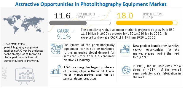
The Photolithography Equipment Market in the current year (2022), is expected was valued at USD 11.6 billion and is projected to reach USD 18.0 billion by 2025; it is expected to grow at a CAGR of 9.1%.
The key factors driving the growth of market include the advent of advanced semiconductor manufacturing technologies and the increased government support for carrying out these advancements. The key players in photolithography equipment industry are focusing on research and development activities.
To know about the assumptions considered for the study, Request for Free Sample Report
Market for EUV is expected to grow at the fastest CAGR during forecast period
Based on type, the photolithography equipment market has been segmented into DUV and EUV. These equipment use different light sources to generate different wavelengths that are used for manufacturing semiconductor devices. Advancements in artificial intelligence (AI), the Internet of Things (IoT), and 5G are expected to boost the demand for EUV photolithography. The adoption of EUV photolithography equipment reduces the requirement of re-engineering each new process, thereby enabling 7 nm and 5 nm processes (and their successors) to share design rules. This approach is expected to significantly reduce the transition time of new geometries, thereby resulting in new options and opportunities for customers in the marketplace.
70 nm–1 nm segment to account for largest share of photolithography equipment market in 2025
Based on wavelength, the market has been segmented into 370 nm–270 nm, 270 nm–170 nm, and 70 nm–1 nm. The 70 nm–1 nm wavelength is the most improved wavelength range used for manufacturing semiconductor devices, such as ICs, transistors, and memories. As such, the 70 nm–1 nm segment of the photolithography equipment market analysis is projected to grow at the highest CAGR during the forecast period. This wavelength is used for manufacturing negative AND (NAND) logic gates and dynamic random-access memory (DRAM). It enables semiconductor manufacturers to produce memory chips at low costs. Among different types of photolithography equipment industry used, EUV photolithography equipment use this wavelength to manufacture semiconductor devices.
Laser-produced plasmas segment to account for the largest size of photolithography equipment market in 2025
Based on light source, market has been classified into mercury lamps, excimer lasers, fluorine lasers, and laser-produced plasmas. The flourishing market for EUV photolithography equipment drives the demand for laser-produced plasma light sources. Laser-produced plasmas are preferred in newly introduced EUV photolithography equipment. They offer highly improved wavelengths of up to 1 nm. These plasmas act as cold UV light sources and offer monochromic light with a bandwidth of 10 nm. The LED used in EUV photolithography equipment is of low cost, requires less power, and has a longer lifespan than other light sources.
APAC to account for a significant market share during the forecast period
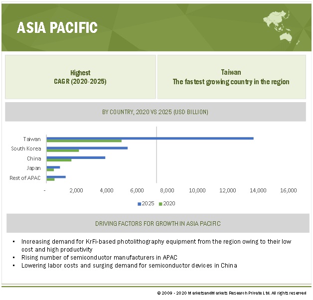
The photolithography equipment market in APAC is projected to grow at the highest CAGR from 2020 to 2025. In this region, countries such as China, Taiwan, Japan, and South Korea have a number of semiconductor foundries. China, Taiwan, and South Korea are projected to be the leading countries in terms of semiconductor spending in 2021. Increasing investments for the development of foundries and memories in China are expected to establish the country as a leading market in the world during the forecast period.
To know about the assumptions considered for the study, download the pdf brochure
Key Market Players
The photolithography equipment companies profiled in this report ASML (Netherland), Canon (Japan), Nikon (Japan), NuFlare Technology (Japan), Onto Innovations (US), Veeco Instrument (US), SUSS Microtek (Germany), NXQ (US), EV Group (US).
Scope of Report
|
Report Metric |
Details |
| Market size value in 2022 | USD 11.6 Billion |
| Market size value in 2025 | USD 18.0 Billion |
| Growth rate | CAGR of 9.1% |
|
Market size available for years |
2015–2025 |
|
Base year considered |
2019 |
|
Forecast period |
2020–2025 |
|
Forecast units |
Value (USD Billion and USD Million) |
|
Segments covered |
By Type, By Wavelength, By Light Source, By End User |
|
Geographies covered |
Asia Pacific, Europe, North America, RoW |
|
Companies covered |
The major market players include are ASML (Netherland), Canon (Japan), Nikon (Japan), NuFlare Technology (Japan), Onto Innovations (US), Veeco Instrument (US), SUSS Microtek (Germany), NXQ (US), EV Group (US). |
The study categorizes the photolithography equipment market based on type, wavelength, light source, end user, regional and global analysis.
By Type
- EUV
- DUV
- I-Line
- ArF
- ArFi
- KrF
By Wavelength
- 370 nm–270 nm
- 270 nm–170 nm
- 70 nm–1 nm
By Wavelength
- Mercury Lamps
- Fluorine Lasers
- Excimer Lasers
- Lased-Produced Plasma
By End User
- IDMs
- Foundries
By Region
- North America
- Europe
- APAC
- Rest of the World
Recent Developments
- In 2020, Taiwan Semiconductor Manufacturing Co. (TSMC) announced that ~50% of all EUV lithography systems installed and operational worldwide are supplied by it. In November 2020, TSMC placed orders for 13 EUV systems with ASML. These systems are expected to be delivered throughout 2021, though the exact delivery and installation schedule is unknown. Meanwhile, the actual requirements of TSMC for the next year might be as high as 16–17 EUV scanners as the company is ramping-up production of chips using its fabrication technologies that feature EUV layers.
- In July 2020, Canon Inc. launched FPA-8000iW, the first Canon semiconductor lithography system to support manufacturing using large panels that are common in back-end processing.
- In April 2019, Nikon Corporation launched an optical processing machine Lasermeister 100A. It is Nikon’s proprietary metal processing machine that performs various metal processing with ease using a laser. Its capability encompasses additive manufacturing as a 3D printer, laser marking, and welding. The advanced optical technology and precision control technology developed for Nikon’s lithography systems enables them to realize a high-quality, smaller sized, and less expensive processing machine.
Frequently Asked Questions (FAQ):
How the adoption of photolithography driving the semiconductor industry?
Growing investments in wireless technologies such as 5G have opened new opportunities for smartphone OEMs to tap the potential of low-latency augmented reality (AR), virtual reality (VR), and live video streaming applications. This is leading to the development of high-performance and multifunctional ICs. As transistor density increases in ICs, the demand for photolithography equipment for manufacturing these high-density ICs is also growing. This, in turn, is leading to increased investments for the construction of new fabrication facilities and expansion of existing ones to meet the surging demand for ICs.
What are the typical use cases of photolithography equipment market across various consumer electronics industry?
As semiconductor designs are constantly shrinking in terms of size, EUV photolithography equipment has become very critical. These equipment allow the development of intricate patterns on semiconductor wafers required for the next-generation AI, 5G, and automotive applications. Increasing customer confidence in EUV photolithography equipment is translating to an increased number of layers in logic production, as well as the surged adoption of these equipment in new markets. ASML expects increased demand for EUV photolithography equipment in the future and anticipates a surged order flow to continue in the coming years
Which are the driving factors for the photolithography equipment market growth?
The key factors driving the growth of the photolithography equipment market include the advent of advanced semiconductor manufacturing technologies and the increased government support for carrying out these advancements. The key players in the market are focusing on research and development activities. They are launching new technologies to improve the photolithography process used for the manufacturing of semiconductor devices. .
To speak to our analyst for a discussion on the above findings, click Speak to Analyst

TABLE OF CONTENTS
1 INTRODUCTION (Page No. - 22)
1.1 STUDY OBJECTIVES
1.2 DEFINITION
1.2.1 INCLUSIONS AND EXCLUSIONS
1.3 STUDY SCOPE
1.3.1 MARKETS COVERED
FIGURE 1 PHOTOLITHOGRAPHY EQUIPMENT MARKET
1.3.2 GEOGRAPHIC SCOPE
1.3.3 YEARS CONSIDERED
1.4 CURRENCY
1.5 LIMITATIONS
1.6 STAKEHOLDERS
1.7 SUMMARY OF CHANGES
2 RESEARCH METHODOLOGY (Page No. - 26)
2.1 RESEARCH DATA
FIGURE 2 MARKET: RESEARCH DESIGN
2.1.1 SECONDARY AND PRIMARY RESEARCH
2.1.2 SECONDARY DATA
2.1.2.1 Secondary sources
2.1.3 PRIMARY DATA
2.1.3.1 Primary sources
2.1.3.2 Key industry insights
2.1.3.3 Breakdown of primaries
2.2 MARKET SIZE ESTIMATION
FIGURE 3 MARKET SIZE ESTIMATION METHODOLOGY
2.2.1 BOTTOM-UP APPROACH
FIGURE 4 BOTTOM-UP APPROACH: MARKET SIZE ESTIMATION METHODOLOGY
2.2.2 TOP-DOWN APPROACH
FIGURE 5 BOTTOM-UP APPROACH: MARKET SIZE ESTIMATION METHODOLOGY
2.3 MARKET BREAKDOWN AND DATA TRIANGULATION
FIGURE 6 DATA TRIANGULATION
2.4 RESEARCH ASSUMPTIONS
3 EXECUTIVE SUMMARY (Page No. - 36)
FIGURE 7 TOP 3 PLAYERS IN PHOTOLITHOGRAPHY EQUIPMENT INDUSTRY FROM 2017 TO 2025
FIGURE 8 EUV SEGMENT TO HOLD LARGE SHARE OF MARKET IN 2025
FIGURE 9 70 NM–1 NM SEGMENT TO ACCOUNT FOR LARGEST SHARE OF MARKET IN 2025
FIGURE 10 LASER-PRODUCED PLASMAS SEGMENT TO ACCOUNT FOR LARGEST SIZE OF MARKET IN 2025
FIGURE 11 MARKET IN APAC TO GROW AT HIGHEST CAGR FROM 2020 TO 2025
4 PREMIUM INSIGHTS (Page No. - 41)
4.1 ATTRACTIVE OPPORTUNITIES IN MARKET
FIGURE 12 INCREASED GLOBAL DEMAND FOR SEMICONDUCTOR CHIPS FOR USE IN CONSUMER ELECTRONICS FUELS GROWTH OF MARKET
4.2 MARKET, BY TYPE
FIGURE 13 EUV SEGMENT TO ACCOUNT FOR LARGE SHARE OF MARKET IN 2025
4.3 MARKET, BY WAVELENGTH
FIGURE 14 70 NM–1 NM SEGMENT TO ACCOUNT FOR LARGEST SIZE OF MARKET FROM 2017 TO 2025
4.4 MARKET, BY LIGHT SOURCE
FIGURE 15 LASER-PRODUCED PLASMAS SEGMENT TO ACCOUNT FOR LARGEST SIZE OF MARKET IN 2025
4.5 MARKET, BY END USER
FIGURE 16 FOUNDRIES SEGMENT TO ACCOUNT FOR LARGE SHARE OF MARKET IN 2020 AND 2025
4.6 MARKET, BY REGION
FIGURE 17 APAC TO HOLD LARGEST SIZE OF MARKET FROM 2020 TO 2025
5 MARKET OVERVIEW (Page No. - 44)
5.1 INTRODUCTION
5.2 MARKET DYNAMICS
FIGURE 18 PHOTOLITHOGRAPHY EQUIPMENT MARKET DYNAMICS
5.2.1 DRIVERS
5.2.1.1 Surged demand for semiconductor devices across several industries
FIGURE 19 GLOBAL SEMICONDUCTOR MARKET GROWTH FROM 2018 TO 2025
5.2.1.2 Advent of advanced technologies for semiconductor device manufacturing
5.2.1.3 Increased government support to companies operating in photolithography equipment market
FIGURE 20 IMPACT OF DRIVERS ON MARKET
5.2.2 RESTRAINTS
5.2.2.1 Functional defects in photolithography equipment and feature pattern complexity during manufacturing process
5.2.2.2 Lack of technical expertise to operate EUV photolithography equipment
5.2.2.3 High costs of photolithography equipment
TABLE 1 EUV PHOTOLITHOGRAPHY EQUIPMENT PRICING ANALYSIS, 2016–2025 (USD MILLION)
FIGURE 21 IMPACT OF RESTRAINTS ON MARKET
5.2.3 OPPORTUNITIES
5.2.3.1 Growth of advanced packaging market across the world
FIGURE 22 IMPACT OF OPPORTUNITIES ON PHOTOLITHOGRAPHY EQUIPMENT MARKET
5.2.4 CHALLENGES
5.2.4.1 Technical difficulties faced in fabrication of ICs
5.2.4.2 Limited reliability of exposure tools
5.2.4.3 Chances of mask contamination
FIGURE 23 IMPACT OF CHALLENGES ON MARKET
5.3 VALUE CHAIN ANALYSIS
FIGURE 24 MARKET: VALUE CHAIN ANALYSIS
5.4 PORTER FIVE FORCE ANALYSIS
TABLE 2 IMPACT OF PORTER’S FIVE FORCES ON MARKET, 2019–2025
5.5 PRICING ANALYSIS
FIGURE 25 PRICING ANALYSIS FOR EUV PHOTOLITHOGRAPHY EQUIPMENT, 2016–2025 (USD MILLION)
FIGURE 26 PRICING ANALYSIS FOR DUV PHOTOLITHOGRAPHY EQUIPMENT, 2016–2025 (USD MILLION)
5.6 TRADE ANALYSIS
TABLE 3 IMPORT DATA OF MACHINES AND APPARATUSES USED FOR MANUFACTURING SEMICONDUCTOR DEVICES OR ELECTRONIC INTEGRATED CIRCUITS, BY COUNTRY, 2015–2019 (USD MILLION)
TABLE 4 EXPORT DATA OF MACHINES AND APPARATUSES USED FOR MANUFACTURING SEMICONDUCTOR DEVICES OR ELECTRONIC INTEGRATED CIRCUITS, BY COUNTRY, 2015–2019 (USD MILLION)
5.7 ECOSYSTEM ANALYSIS
5.8 CASE STUDIES/USE CASES
5.8.1 VA-Q-TEC PARTNERED WITH ASML FOR RISK ASSESSMENT OF TEMPERATURE PROFILES ON ROUTES OF ASML
5.8.2 LAM RESEARCH UNVEILS TECHNOLOGY BREAKTHROUGH FOR EUV LITHOGRAPHY
5.8.3 TSMC PLACES ORDER FOR EUV SYSTEMS WITH ASML TO BOOST ITS CHIP PRODUCTION CAPACITY
5.8.4 SAMSUNG ELECTRONICS STARTED MASS PRODUCTION OF 7 NM AND 6 NM CHIPS
5.9 PATENT ANALYSIS
5.10 TECHNOLOGY ANALYSIS
TABLE 5 PHOTOLITHOGRAPHY TECHNOLOGIES
5.11 REGULATORY STANDARDS
5.11.1 RESTRICTION OF HAZARDOUS SUBSTANCES (ROHS) AND WASTE ELECTRICAL AND ELECTRONIC EQUIPMENT (WEEE)
5.11.2 REGISTRATION, EVALUATION, AUTHORIZATION, AND RESTRICTION OF CHEMICALS (REACH)
5.11.3 UN FRAMEWORKS TO ADDRESS GLOBAL ISSUES RELATED TO ENVIRONMENT
5.12 CODES AND STANDARDS
TABLE 6 MANDATORY CODES & STANDARDS IN SEMICONDUCTOR INDUSTRY
6 PHOTOLITHOGRAPHY EQUIPMENT MARKET, BY TYPE (Page No. - 64)
6.1 INTRODUCTION
FIGURE 27 MARKET, BY TYPE, 2020 & 2025
TABLE 7 MARKET, BY TYPE, 2015–2019 (USD MILLION)
TABLE 8 MARKET, BY TYPE, 2020–2025 (USD MILLION)
TABLE 9 MARKET, BY TYPE, 2015–2019 (UNITS)
TABLE 10 MARKET, BY TYPE, 2020–2025 (UNITS)
TABLE 11 PHOTOLITHOGRAPHY EQUIPMENT SHIPMENTS OF ASML, BY TYPE, 2015–2019 (UNITS)
FIGURE 28 SHIPMENTS OF EUV PHOTOLITHOGRAPHY EQUIPMENT OF ASML TO GROW AT HIGHEST CAGR FROM 2020 TO 2025
TABLE 12 PHOTOLITHOGRAPHY EQUIPMENT SHIPMENTS OF ASML, BY TYPE, 2020–2025 (UNITS)
TABLE 13 PHOTOLITHOGRAPHY EQUIPMENT SHIPMENTS OF CANON, BY TYPE, 2015–2019 (UNITS)
TABLE 14 PHOTOLITHOGRAPHY EQUIPMENT SHIPMENTS OF CANON, BY TYPE, 2020–2025 (UNITS)
TABLE 15 PHOTOLITHOGRAPHY EQUIPMENT SHIPMENTS OF NIKON, BY TYPE, 2015–2019 (UNITS)
TABLE 16 PHOTOLITHOGRAPHY EQUIPMENT SHIPMENTS OF NIKON, BY TYPE, 2020–2025 (UNITS)
6.2 EUV
6.2.1 INCREASED USE OF EUV PHOTOLITHOGRAPHY FOR MANUFACTURING COMPUTER CHIPS BEYOND CURRENT 193 NM-BASED OPTICAL LITHOGRAPHY
TABLE 17 EUV MARKET, BY WAVELENGTH, 2015–2019 (USD MILLION)
TABLE 18 EUV MARKET, BY WAVELENGTH, 2020–2025 (USD MILLION)
TABLE 19 EUV PHOTOLITHOGRAPHY EQUIPMENT MARKET, BY LIGHT SOURCE, 2015–2019 (USD MILLION)
TABLE 20 EUV MARKET, BY LIGHT SOURCE, 2020–2025 (USD MILLION)
6.3 DUV
TABLE 21 DUV MARKET, BY EQUIPMENT TYPE, 2015–2019 (USD MILLION)
TABLE 22 DUV MARKET, BY EQUIPMENT TYPE, 2020–2025 (USD MILLION)
TABLE 23 DUV MARKET, BY EQUIPMENT TYPE, 2015–2019 (UNITS)
FIGURE 29 I-LINE SEGMENT TO ACCOUNT FOR LARGEST SIZE OF DUV MARKET IN 2020
TABLE 24 DUV PHOTOLITHOGRAPHY EQUIPMENT MARKET, BY EQUIPMENT TYPE, 2020–2025 (UNITS)
6.3.1 I-LINE
6.3.1.1 Low-cost of i-line DUV photolithography equipment leads to their increased global adoption
TABLE 25 I-LINE DUV MARKET, BY WAVELENGTH, 2015–2019 (USD MILLION)
TABLE 26 I-LINE DUV MARKET, BY WAVELENGTH, 2020–2025 (USD MILLION)
TABLE 27 I-LINE DUV MARKET, BY LIGHT SOURCE, 2015–2019 (USD MILLION)
TABLE 28 I-LINE DUV PHOTOLITHOGRAPHY EQUIPMENT ANALYSIS MARKET, BY LIGHT SOURCE, 2020–2025 (USD MILLION)
6.3.2 KRF
6.3.2.1 Surged use of KrF lithography in high-resolution photolithography equipment
TABLE 29 KRF DUV MARKET, BY WAVELENGTH, 2015–2019 (USD MILLION)
TABLE 30 KRF DUV MARKET, BY WAVELENGTH, 2020–2025 (USD MILLION)
TABLE 31 KRF DUV MARKET, BY LIGHT SOURCE, 2015–2019 (USD MILLION)
FIGURE 30 EXCIMER LASERS SEGMENT OF KRF DUV PHOTOLITHOGRAPHY EQUIPMENT MARKET TO GROW AT SIGNIFICANT RATE FROM 2020 TO 2025
TABLE 32 KRF DUV MARKET, BY LIGHT SOURCE, 2020–2025 (USD MILLION)
6.3.3 ARF
6.3.3.1 Risen adoption of DUV ArFi photolithography by chip manufacturers to address requirements of 10 nm device nodes
TABLE 33 ARF DUV MARKET, BY WAVELENGTH, 2015–2019 (USD MILLION)
TABLE 34 ARF DUV MARKET, BY WAVELENGTH, 2020–2025 (USD MILLION)
TABLE 35 ARF DUV MARKET, BY LIGHT SOURCE, 2015–2019 (USD MILLION)
TABLE 36 ARF DUV MARKET, BY LIGHT SOURCE, 2020–2025 (USD MILLION)
6.3.4 ARFI
6.3.4.1 ArFi segment contributes significantly to growth of DUV photolithography equipment market globally
TABLE 37 ARFI DUV MARKET, BY WAVELENGTH, 2015–2019 (USD MILLION)
TABLE 38 ARFI DUV MARKET, BY WAVELENGTH, 2020–2025 (USD MILLION)
TABLE 39 ARFI DUV MARKET, BY LIGHT SOURCE, 2015–2019 (USD MILLION)
TABLE 40 ARFI DUV MARKET, BY LIGHT SOURCE, 2020–2025 (USD MILLION)
7 PHOTOLITHOGRAPHY EQUIPMENT MARKET, BY WAVELENGTH (Page No. - 81)
7.1 INTRODUCTION
FIGURE 31 MARKET, BY WAVELENGTH, 2020 & 2025
TABLE 41 MARKET, BY WAVELENGTH, 2015–2019 (USD MILLION)
TABLE 42 MARKET, BY WAVELENGTH, 2020–2025 (USD MILLION)
7.2 370 NM–270 NM
7.2.1 I-LINE PHOTOLITHOGRAPHY EQUIPMENT USE 370 NM–270 NM WAVELENGTH TO MANUFACTURE SEMICONDUCTOR DEVICES
TABLE 43 MARKET FOR 370 NM–270 NM WAVELENGTH, BY TYPE, 2015–2019 (USD MILLION)
TABLE 44 MARKET FOR 370 NM–270 NM WAVELENGTH, BY TYPE, 2020–2025 (USD MILLION)
7.3 270 NM–170 NM WAVELENGTH
7.3.1 INCREASED ADOPTION OF 270 NM–170 NM WAVELENGTH IN KRF AND ARF PHOTOLITHOGRAPHY
TABLE 45 MARKET FOR 270 NM–170 NM WAVELENGTH, BY TYPE, 2015–2019 (USD MILLION)
FIGURE 32 ARFI SEGMENT TO HOLD LARGEST SIZE OF PHOTOLITHOGRAPHY EQUIPMENT MARKET FOR 270 NM–170 NM WAVELENGTH FROM 2020 TO 2025
TABLE 46 MARKET FOR 270 NM–170 NM WAVELENGTH, BY TYPE, 2020–2025 (USD MILLION)
7.4 70 NM–1 NM WAVELENGTH
7.4.1 SURGED DEMAND FOR EUV PHOTOLITHOGRAPHY EQUIPMENT TO DRIVE GROWTH OF 70 NM–1 NM WAVELENGTH SEGMENT OF MARKET FROM 2020 TO 2025
TABLE 47 MARKET FOR 70 NM–1 NM WAVELENGTH, BY TYPE, 2015–2019 (USD MILLION)
TABLE 48 MARKET FOR 70 NM–1 NM WAVELENGTH, BY TYPE, 2020–2025 (USD MILLION)
8 PHOTOLITHOGRAPHY EQUIPMENT MARKET, BY LIGHT SOURCE (Page No. - 88)
8.1 INTRODUCTION
FIGURE 33 MARKET, BY LIGHT SOURCE, 2020 & 2025
TABLE 49 MARKET, BY LIGHT SOURCE, 2015–2019 (USD MILLION)
TABLE 50 MARKET, BY LIGHT SOURCE, 2020–2025 (USD MILLION)
8.2 MERCURY LAMPS
8.2.1 MERCURY LAMPS GENERATE DIFFERENT WAVELENGTHS SIMULTANEOUSLY
TABLE 51 MERCURY LAMP-BASED MARKET, BY TYPE, 2015–2019 (USD MILLION)
TABLE 52 MERCURY LAMP-BASED MARKET, BY TYPE, 2020–2025 (USD MILLION)
8.3 EXCIMER LASERS
8.3.1 INCREASED USE OF EXCIMER LASERS FOR MANUFACTURING SEMICONDUCTOR CHIPS AND MICRO STRUCTURING OF GLASS AND PLASTICS
TABLE 53 EXCIMER LASER-BASED MARKET, BY TYPE, 2015–2019 (USD MILLION)
FIGURE 34 ARFI SEGMENT TO HOLD LARGEST SIZE OF EXCIMER LASER-BASED PHOTOLITHOGRAPHY EQUIPMENT MARKET ANALYSIS FROM 2020 TO 2025
TABLE 54 EXCIMER LASER-BASED MARKET, BY TYPE, 2020–2025 (USD MILLION)
8.4 FLUORINE LASERS
8.4.1 SURGED USE OF FLUORINE LASERS AT 193 NM WAVELENGTH FOR ARF IMMERSION (ARFI)
TABLE 55 FLUORINE LASER-BASED MARKET, BY TYPE, 2015–2019 (USD MILLION)
TABLE 56 FLUORINE LASER-BASED MARKET, BY TYPE, 2020–2025 (USD MILLION)
8.5 LASER-PRODUCED PLASMAS
8.5.1 RISEN GLOBAL DEMAND FOR EUV PHOTOLITHOGRAPHY EQUIPMENT MARKET CONTROL OUTLOOK REVENUE FUELS GROWTH OF LASER-PRODUCED PLASMAS SEGMENT OF MARKET
TABLE 57 LASER-PRODUCED PLASMA-BASED MARKET, BY TYPE, 2015–2019 (USD MILLION)
TABLE 58 LASER-PRODUCED PLASMA-BASED PHOTOLITHOGRAPHY EQUIPMENT MARKET, BY TYPE, 2020–2025 (USD MILLION)
9 MARKET, BY END USER (Page No. - 95)
9.1 INTRODUCTION
FIGURE 35 FOUNDRIES SEGMENT TO LEAD MARKET FROM 2020 TO 2025
TABLE 59 MARKET, BY END USER, 2015–2019 (USD BILLION)
TABLE 60 MARKET, BY END USER, 2020–2025 (USD BILLION)
9.2 INTEGRATED DEVICE MANUFACTURERS
9.2.1 INCREASED SPENDING OF INTEGRATED DEVICE MANUFACTURERS FOR IN-HOUSE MANUFACTURING OF INTEGRATED CIRCUITS FUELS MARKET GROWTH
9.3 FOUNDRIES
9.3.1 LARGE-SCALE ADOPTION OF EUV PHOTOLITHOGRAPHY-BASED EQUIPMENT BY FOUNDRIES
10 GEOGRAPHIC ANALYSIS (Page No. - 100)
10.1 INTRODUCTION
FIGURE 36 GEOGRAPHIC SNAPSHOT OF PHOTOLITHOGRAPHY EQUIPMENT MARKET FROM 2020 TO 2025
TABLE 61 MARKET, BY REGION, 2015–2019 (USD MILLION)
TABLE 62 MARKET, BY REGION, 2020–2025 (USD MILLION)
10.2 NORTH AMERICA
FIGURE 37 SNAPSHOT OF MARKET IN NORTH AMERICA
TABLE 63 MARKET IN NORTH AMERICA, BY COUNTRY, 2015–2019 (USD MILLION)
TABLE 64 MARKET IN NORTH AMERICA, BY COUNTRY, 2020–2025 (USD MILLION)
10.2.1 US
10.2.1.1 US to be largest market for photolithography equipment in North America from 2020 to 2025
10.2.2 OTHERS
10.3 EUROPE
FIGURE 38 SNAPSHOT OF MARKET IN EUROPE
TABLE 65 MARKET IN EUROPE, BY COUNTRY, 2015–2019 (USD MILLION)
TABLE 66 MARKET IN EUROPE, BY COUNTRY, 2020–2025 (USD MILLION)
10.3.1 GERMANY
10.3.1.1 Germany projected to be largest electronics manufacturer in Europe from 2020 to 2025
10.3.2 ISRAEL
10.3.2.1 Intel invested USD 5.0 billion in expanding its Kiryat Gat production plant in Israel
10.3.3 FRANCE
10.3.3.1 Increased demand for semiconductor devices drive the growth of photolithography equipment market in France
10.3.4 ITALY
10.3.4.1 Growth of IoT market in Italy to fuel demand for semiconductors in-country
10.3.5 NETHERLANDS
10.3.5.1 Presence of ASML in Netherlands
10.4 APAC
TABLE 67 SEMICONDUCTOR COMPANIES IN APAC
FIGURE 39 SNAPSHOT OF PHOTOLITHOGRAPHY EQUIPMENT MARKET IN APAC
TABLE 68 MARKET IN APAC, BY COUNTRY, 2015–2019 (USD MILLION)
TABLE 69 MARKET IN APAC, BY COUNTRY, 2020–2025 (USD MILLION)
10.4.1 CHINA
10.4.1.1 Accelerated efforts in China to make its domestic semiconductors industry self-reliant
10.4.2 SOUTH KOREA
10.4.2.1 Increased number of patents related to photolithography filed by companies based in South Korea to boost market growth
10.4.3 JAPAN
10.4.3.1 Advancements in EUV testing to fuel market growth in Japan
10.4.4 TAIWAN
10.4.4.1 TSMC drives the growth of market in Taiwan
10.4.5 REST OF APAC
10.5 REST OF THE WORLD (ROW)
11 COMPETITIVE LANDSCAPE (Page No. - 114)
11.1 OVERVIEW
11.2 REVENUE ANALYSIS OF TOP 3 PLAYERS
FIGURE 40 ASML DOMINATED PHOTOLITHOGRAPHY EQUIPMENT MARKET FROM 2015 TO 2019
TABLE 70 NEW EQUIPMENT SALES OF ASML, 2000–2010 (UNITS)
TABLE 71 NEW EQUIPMENT SALES OF ASML, 2011–2019 (UNITS)
TABLE 72 NEW EQUIPMENT SALES OF ASML, 2020–2025 (UNITS)
TABLE 73 CUMULATIVE NEW EQUIPMENT SALES OF ASML, 2015–2019 (UNITS)
TABLE 74 CUMULATIVE NEW EQUIPMENT SALES OF ASML, 2020–2025 (UNITS)
TABLE 75 NEW EQUIPMENT SALES OF CANON, 2000–2010 (UNITS)
TABLE 76 NEW EQUIPMENT SALES OF CANON, 2011–2019 (UNITS)
TABLE 77 NEW EQUIPMENT SALES OF CANON, 2020–2025 (UNITS)
TABLE 78 CUMULATIVE NEW EQUIPMENT SALES OF CANON, 2015–2019 (UNITS)
TABLE 79 CUMULATIVE NEW EQUIPMENT SALES OF CANON, 2020–2025 (UNITS)
TABLE 80 NEW EQUIPMENT SALES OF NIKON, 2000–2010 (UNITS)
TABLE 81 NEW EQUIPMENT SALES OF NIKON, 2011–2019 (UNITS)
TABLE 82 NEW EQUIPMENT SALES OF NIKON, 2020–2025 (UNITS)
TABLE 83 CUMULATIVE NEW EQUIPMENT SALES OF NIKON, 2015–2019 (UNITS)
TABLE 84 CUMULATIVE NEW EQUIPMENT SALES OF NIKON, 2020–2025 (UNITS)
11.3 PHOTOLITHOGRAPHY EQUIPMENT MARKET CONTROL OUTLOOK REVENUE SHARE ANALYSIS, 2019
FIGURE 41 TOP 3 PLAYERS DOMINATED MARKET IN 2019
TABLE 85 LIST OF FABRICATION FACILITIES OF SAMSUNG
TABLE 86 LIST OF FABRICATION FACILITIES OF TSMC
TABLE 87 LIST OF FABRICATION FACILITIES OF GLOBAL FOUNDRIES
TABLE 88 LIST OF FABRICATION FACILITIES OF UMC
TABLE 89 LIST OF FABRICATION FACILITIES OF SMIC
TABLE 90 LITHOGRAPHY TECHNOLOGY ADOPTION BY MAJOR FOUNDRIES
11.4 COMPANY EVALUATION MATRIX
11.4.1 STAR
11.4.2 PERVASIVE
11.4.3 EMERGING LEADER
11.4.4 PARTICIPANT
FIGURE 42 PHOTOLITHOGRAPHY EQUIPMENT MARKET (GLOBAL) COMPANY EVALUATION QUADRANT, 2019
11.4.5 PRODUCT FOOTPRINT ANALYSIS OF TOP PLAYERS
TABLE 91 PRODUCT FOOTPRINT OF COMPANIES
TABLE 92 REGIONAL FOOTPRINT OF COMPANIES
11.5 COMPETITIVE SITUATIONS AND TRENDS
TABLE 93 MARKET: PRODUCT LAUNCHES AND DEVELOPMENTS
TABLE 94 MARKET: AGREEMENTS
12 COMPANY PROFILES (Page No. - 127)
12.1 KEY PLAYERS
(Business Overview, Products/Solutions/Services Offered, Recent Developments, and MnM View)*
12.1.1 ASML HOLDING N.V.
FIGURE 43 ASML HOLDING N.V.: COMPANY SNAPSHOT
12.1.2 NIKON CORPORATION
FIGURE 44 NIKON CORPORATION: COMPANY SNAPSHOT
12.1.3 CANON INC.
FIGURE 45 CANON, INC.: COMPANY SNAPSHOT
12.1.4 NUFLARE TECHNOLOGY INC.
FIGURE 46 NUFLARE TECHNOLOGY INC.: COMPANY SNAPSHOT
12.1.5 ONTO INNOVATION INC.
FIGURE 47 OTNO INNOVATION INC.: COMPANY SNAPSHOT
12.1.6 VEECO INSTRUMENTS INC.
FIGURE 48 VEECO INSTRUMENTS INC.: COMPANY SNAPSHOT
12.1.7 SUSS MICROTEC AG
FIGURE 49 SUSS MICROTEC AG: COMPANY SNAPSHOT
12.1.8 NEUTRONIX QUINTEL
12.1.9 EV GROUP
12.1.10 EULITHA AG
12.1.11 NIL TECHNOLOGY
* Business Overview, Products/Solutions/Services Offered, Recent Developments, and MnM View might not be captured in case of unlisted companies.
13 ADJACENT & RELATED MARKETS (Page No. - 152)
13.1 INTRODUCTION
13.2 LIMITATIONS
13.3 SEMICONDUCTOR MANUFACTURING EQUIPMENT MARKET
13.3.1 MARKET DEFINITION
13.3.2 MARKET OVERVIEW
13.4 SEMICONDUCTOR MANUFACTURING EQUIPMENT MARKET, BY PRODUCT TYPE
TABLE 95 SEMICONDUCTOR MANUFACTURING EQUIPMENT MARKET, BY PRODUCT, 2016–2019 (USD BILLION)
TABLE 96 SEMICONDUCTOR MANUFACTURING EQUIPMENT MARKET, BY PRODUCT, 2020–2025 (USD BILLION)
13.5 SEMICONDUCTOR MANUFACTURING EQUIPMENT MARKET, BY SUPPLY CHAIN PARTICIPANTS
TABLE 97 SEMICONDUCTOR MANUFACTURING EQUIPMENT MARKET, BY SUPPLY CHAIN PARTICIPANT, 2016-2019 (USD BILLION)
TABLE 98 SEMICONDUCTOR MANUFACTURING EQUIPMENT MARKET, BY SUPPLY CHAIN PARTICIPANT, 2020–2025 (USD BILLION)
13.6 SEMICONDUCTOR MANUFACTURING EQUIPMENT MARKET, BY REGION
TABLE 99 SEMICONDUCTOR MANUFACTURING EQUIPMENT MARKET, BY REGION, 2016–2019 (USD BILLION)
TABLE 100 SEMICONDUCTOR MANUFACTURING EQUIPMENT MARKET, BY REGION, 2020–2025 (USD BILLION)
14 APPENDIX (Page No. - 157)
14.1 INSIGHTS FROM INDUSTRY EXPERTS
14.2 DISCUSSION GUIDE
14.3 KNOWLEDGE STORE: MARKETSANDMARKETS’ SUBSCRIPTION PORTAL
14.4 AVAILABLE CUSTOMIZATION
14.5 RELATED REPORTS
14.6 AUTHOR DETAILS
The study involved four major activities in estimating the size for photolithography equipment market. Exhaustive secondary research was done to collect information on the market, peer market, and parent market. The next step was to validate these findings, assumptions, and sizing with industry experts across value chains through primary research. The bottom-up approach was employed to estimate the overall market size. After that, market breakdown and data triangulation were used to estimate the market size of segments and subsegments.
Secondary Research
Secondary sources referred to for this research study include corporate filings (such as annual reports, investor presentations, and financial statements); trade, business, and professional associations; white papers; certified publications; articles from recognized authors; directories; and databases. The secondary data have been collected and analyzed to arrive at the overall market size, which has been further validated through primary research.
Primary Research
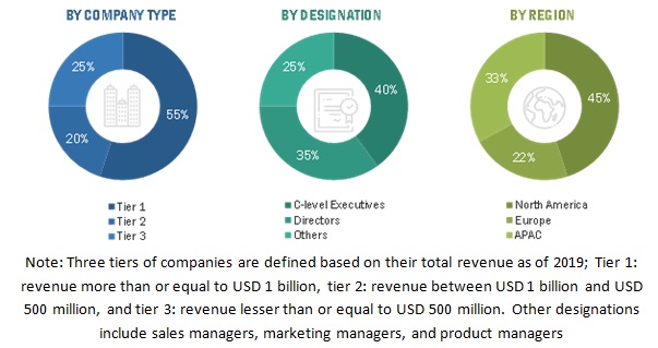
Extensive primary research has been conducted after gaining knowledge about the photolithography equipment market scenario through secondary research. Several primary interviews have been conducted with experts from both demand and supply sides across 4 major regions, namely, North America, Europe, Asia Pacific (APAC), and Rest of the World (RoW). This primary data has been collected through questionnaires, emails, and telephonic interviews. Approximately 70% and 30% of primary interviews have been conducted from the demand and supply side, respectively. Primary data has been collected through questionnaires, emails, and telephonic interviews. In the canvassing of primaries, various departments within organizations, such as sales, operations, and administration, were covered to provide a holistic viewpoint in our report.
After interacting with industry experts, brief sessions were conducted with highly experienced independent consultants to reinforce the findings from our primaries. This, along with the in-house subject matter experts’ opinions, has led us to the findings as described in the remainder of this report.
Following is the breakdown of primary respondents
To know about the assumptions considered for the study, download the pdf brochure
Market Size Estimation
Top-down and bottom-up approaches have been used to estimate and validate the size of the photolithography equipment market and various dependent submarkets. The key players in the market have been identified through secondary research, and their market share in the respective regions has been determined through primary and secondary research.
In the top-down approach, the overall market size has been used to estimate the size of the individual markets (mentioned in the market segmentation) derived through percentage splits from secondary and primary research.
For the calculation of specific market segments, the most appropriate parent market size has been considered to implement the top-down approach. The bottom-up approach has also been implemented for the data extracted from the secondary research to validate the obtained market size of segments.
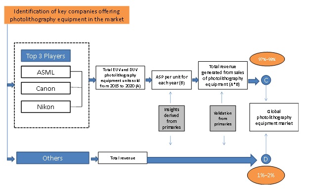
The bottom-up approach has been employed to arrive at the overall size of the photolithography equipment market, in terms of volume, and to determine the average selling price of photolithography equipment products. The multiplication of the number of unit shipments and the average selling price led to the estimation of the overall size of the photolithography equipment market.
Global Photolithography Equipment Market: Top-Down Market Estimation
To know about the assumptions considered for the study, Request for Free Sample Report
Data Triangulation
After arriving at the overall market size from the market size estimation process explained above, the total market has been split into several segments and subsegments. To complete the overall market engineering process and arrive at the exact statistics for all segments and subsegments, the market breakdown and data triangulation procedures have been employed wherever applicable. The data has been triangulated by studying various factors and trends from, both, demand and supply sides. In addition to this, the market size has been validated using both top-down and bottom-up approaches.
Report Objectives
- To define, describe, and forecast the photolithography equipment market based on type, wavelength, end user, and light source
- To forecast the market size for various segments with regard to 4 main regions, namely, North America, Europe, Asia Pacific (APAC), and the Rest of the World (RoW)
- To forecast the market size based on type in terms of volume
- To forecast the shipments of photolithography equipment by different companies from 2020 to 2025
- To provide detailed information regarding the key factors such as drivers, restraints, opportunities, and challenges influencing the growth of the market
- To provide detailed analysis of Porter's five forces, strategic benchmarking of the leading players, and evolution of the photolithography equipment market
- To strategically analyze micromarkets with respect to individual growth trends, prospects, and contributions to the overall market
- To analyze opportunities in the market for stakeholders by identifying high-growth segments of the photolithography equipment market
- To strategically profile the key players and comprehensively analyze their market share and core competencies, along with a detailed competitive landscape for the market leaders
- To study the complete value chain and allied industry segments, as well as perform a value chain analysis of the photolithography equipment landscape
- To track and analyze the competitive developments, such as joint ventures, mergers and acquisitions, new product developments, and research and development activities in the photolithography equipment market
Available Customizations:
With the given market data, MarketsandMarkets offers customizations according to the company’s specific needs. The following customization options are available for this report:
- Additional country-level analysis of photolithography equipment market


 Generating Response ...





Growth opportunities and latent adjacency in Photolithography Equipment Market