Extreme Ultraviolet (EUV) Lithography Market Size, Share and Trends
Extreme Ultraviolet (EUV) Lithography Market by Component (Light Sources, Optics, Masks), System Type (0.33 NA EUV System (NXE), 0.55 NA EUV System (EXE)), Integrated Device Manufacturers, Foundries, Logic Chips, Memory Chips - Global Forecast to 2032


OVERVIEW
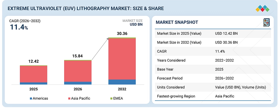
Source: Secondary Research, Interviews with Experts, MarketsandMarkets Analysis
The extreme ultraviolet (EUV) lithography market is expected to grow from USD 15.84 billion in 2026 to USD 30.36 billion in 2032, at a CAGR of 11.4%. The accelerating transition toward leading-edge foundry nodes, including 7 nm, 5 nm, and future technology generations, is a core driver of EUV lithography adoption across the global semiconductor industry. As conventional optical lithography approaches face fundamental limitations in resolution and pattern fidelity at sub-10 nm geometries, EUV lithography has become indispensable for enabling finer features, tighter pitches, and increasingly complex device architectures.
KEY TAKEAWAYS
-
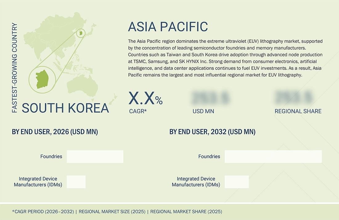
By RegionThe Asia Pacific region accounted for 85.8% market share in 2025.
-
By ComponentBy component, light sources accounted for the largest market share of 53.4% in 2025.
-
By System TypeBy system type, 0.55 NA EUV systems are expected to register the highest CAGR of 28.0% during the forecast period.
-
By End UserBy end user, foundries are expected to record a significant CAGR in the extreme ultraviolet (EUV) lithography market during the forecast period.
-
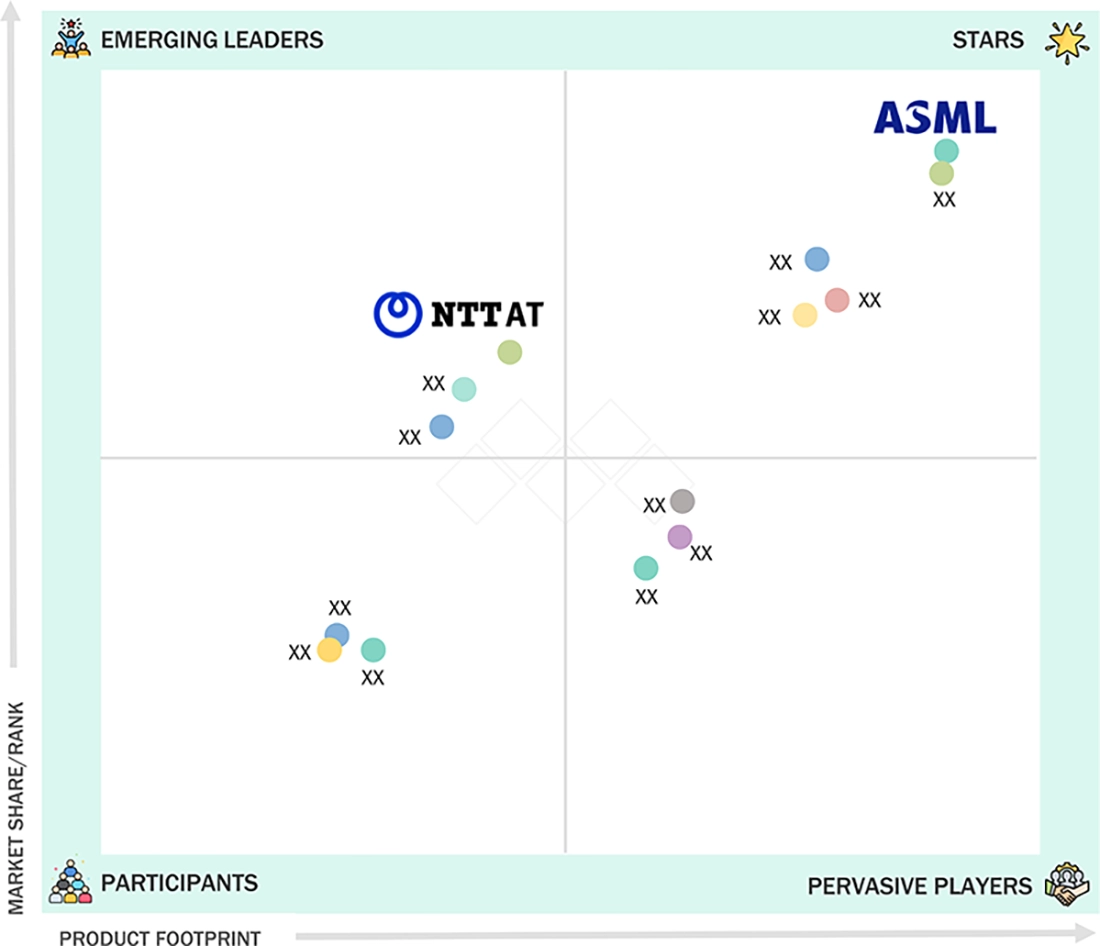
Competitive Landscape - Key PlayersASML, KLA Corporation, ZEISS Group, Lasertec Corporation, TRUMPF, and AGC Inc. were identified as star players in the extreme ultraviolet (EUV) lithography market, given their strong market share, system, and component footprint.
-
Competitive Landscape - Startups and SMEsStartups such as Energetiq, Imagine Optic, EUV Tech, and MLOPTIC Corporation are gaining traction in the extreme ultraviolet (EUV) lithography market as specialized component and subsystem providers. Their growth is driven by increasing demand for high-precision EUV light sources, wavefront sensing solutions, multilayer mirrors, optical metrology, and advanced diagnostic components essential for next-generation semiconductor manufacturing. Additionally, the integration of data analytics, AI-enabled process monitoring, and real-time system diagnostics is enhancing tool performance, uptime, and yield optimization across advanced EUV lithography platforms.
The extreme ultraviolet (EUV) lithography market is driven by the adoption of data-driven technologies, artificial intelligence (AI), and high-performance computing (HPC) applications, which are driving the demand for more advanced and efficient semiconductor solutions. As industries increasingly rely on data analytics, AI, and machine learning (ML) to enhance decision-making and operational efficiency, demand for high-density, high-performance integrated circuits (ICs) is growing. EUV lithography is central to this demand, enabling the production of semiconductors that deliver the computational power and energy efficiency required to support these advanced technologies.
TRENDS & DISRUPTIONS IMPACTING CUSTOMERS' CUSTOMERS
This trend disruption impact illustrates the evolving revenue mix in lithography technologies, showing a shift from traditional sources, including optical and DUV lithography, to EUV lithography, which is driving future growth. This transition is driven by the growing demand for advanced semiconductor nodes (e.g., 3 nm, 5 nm, 7 nm, and 13.5 nm) to meet industry requirements for miniaturization and increased efficiency. Key customers, such as foundries and IDMs, are adopting EUV lithography to enhance semiconductor production capabilities, reflecting how technological advancements are disrupting traditional business models and shaping future strategies.
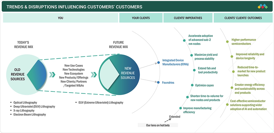
Source: Secondary Research, Interviews with Experts, MarketsandMarkets Analysis
MARKET DYNAMICS
Level
-
Elevating use of AI accelerators and deep learning processors in HPC systems

-
Surging deployment of EUV lithography across leading-edge foundry nodes
Level
-
Need for high capital investment
-
Requirement for advanced infrastructure and skilled workforce
Level
-
Advancements in memory modules and chips
-
Increasing investments in advanced EUV lithography and semiconductor devices
Level
-
Difficulty in sustaining high source power and productivity
-
Detecting and addressing mask defects and yield-related challenges
Source: Secondary Research, Interviews with Experts, MarketsandMarkets Analysis
Driver: Elevating use of AI accelerators and deep learning processors in HPC systems
Rising adoption of AI and high-performance computing is driving demand for advanced, high-density semiconductor chips. EUV lithography enables smaller transistors and tighter interconnects, improving chip speed and energy efficiency. It supports complex processor designs required for AI accelerators and deep learning workloads. EUV also enables high-capacity memory production to handle large data volumes. Together, these capabilities support the performance needs of modern HPC systems.
Restraint: Need for high capital investment
The adoption of EUV lithography requires significant upfront capital investment, primarily because specialized, highly complex equipment and components are required. EUV lithography machines are more expensive than conventional optical lithography systems, presenting a financial barrier, particularly for smaller semiconductor manufacturers or foundries with limited capital. Key components, such as EUV light sources, masks, photoresists, and scanners, are costly to develop, produce, and maintain, thereby contributing to the overall investment required.
Opportunity: Advancements in memory modules and chips
EUV lithography market players are likely to experience growth opportunities due to the increasing focus on developing advanced memory devices. Memory solutions, such as DRAM (Dynamic Random Access Memory) and NAND (Not And) Flash, are integral to the performance of electronic devices such as computers, smartphones, and data center solutions. As the demand for higher capacity, faster, and more energy-efficient memory solutions intensifies, EUV lithography presents a key enabler for the next generation of memory devices.
Challenge: Difficulty in sustaining high source power and productivity
EUV lithography struggles to keep light source power high and stable during production. When power drops, wafer processing slows and fewer chips are produced. This makes it harder to meet high-volume manufacturing needs. Maintaining steady power over long periods is difficult and increases operating challenges. These issues limit production speed and efficiency.
EXTREME ULTRAVIOLET (EUV) LITHOGRAPHY MARKET SIZE, SHARE AND TRENDS: COMMERCIAL USE CASES ACROSS INDUSTRIES
| COMPANY | USE CASE DESCRIPTION | BENEFITS |
|---|---|---|
 |
Uses EUV lithography for advanced logic node manufacturing at 7 nm, 5 nm, and below, enabling high-density transistor patterning for fabless customers across mobile, HPC, and AI markets | Higher transistor density | reduced multi-patterning complexity | improved yield | lower power consumption for advanced logic chips |
 |
Deploys EUV in both logic and DRAM production to fabricate smaller geometries and more complex circuit layouts for mobile processors and memory devices | Enhanced performance per watt | improved memory scaling | reduced process steps| faster time-to-market |
 |
Integrates EUV lithography into next-generation CPU, GPU, and AI accelerator manufacturing to support aggressive node scaling and architectural innovation | Improved process control | higher performance silicon | reduced defect rates | better cost efficiency at advanced nodes |
 |
Uses EUV lithography to manufacture high-density DRAM for data centers, AI servers, and enterprise computing applications | Increased memory capacity per chip | lower power consumption | improved reliability | higher wafer productivity |
 |
Applies EUV to advanced DRAM nodes to simplify patterning steps and support next-generation memory scaling for cloud and edge computing | Lower manufacturing complexity | improved yields | enhanced performance | reduced cost per bit |
Logos and trademarks shown above are the property of their respective owners. Their use here is for informational and illustrative purposes only.
MARKET ECOSYSTEM
The EUV lithography ecosystem consists of a closely linked network of system manufacturers, component suppliers, and semiconductor producers that together enable advanced chip manufacturing. System integrators provide complete EUV exposure tools, while component manufacturers supply critical optics, light sources, masks, metrology, and inspection solutions. End users, including integrated device manufacturers and foundries, rely on this ecosystem to produce smaller, faster, and more efficient chips at advanced technology nodes. Strong coordination across the ecosystem is essential to ensure tool performance, production stability, and scalable semiconductor manufacturing.
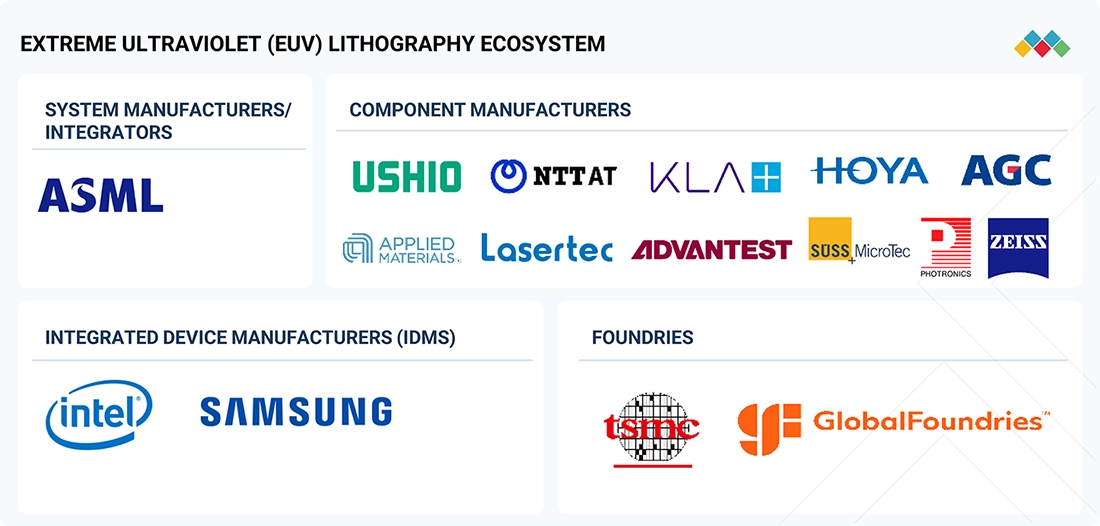
Logos and trademarks shown above are the property of their respective owners. Their use here is for informational and illustrative purposes only.
MARKET SEGMENTS
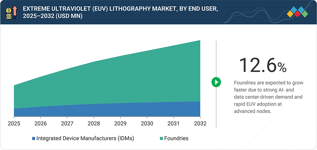
Source: Secondary Research, Interviews with Experts, MarketsandMarkets Analysis
Extreme Ultraviolet (EUV) Lithography Market, By Component
Light sources held the largest share of the extreme ultraviolet (EUV) lithography market, by component, in 2025 due to its critical role in determining tool performance, throughput, and production efficiency. EUV light sources are highly complex, capital-intensive systems that require advanced laser technology, plasma generation, debris mitigation, and precision control, making them the most expensive component within an EUV tool. Continuous demand for higher source power to improve wafer throughput at advanced nodes has driven ongoing upgrades, replacements, and service revenues. In addition, limited supplier availability and long development cycles concentrate spending in this segment, further strengthening its market dominance.
Extreme Ultraviolet (EUV) Lithography Market, By System Type
The 0.33 NA EUV systems (NXE series) held the largest market share in 2025 because they are the most widely deployed platforms in high-volume semiconductor manufacturing. These systems are proven and production-ready, supporting advanced logic and memory nodes with stable performance and high throughput. Most leading chipmakers have standardized their processes around 0.33 NA EUV tools, driving repeat purchases and long-term service contracts. In contrast, higher-NA EUV systems are still in early adoption, keeping 0.33 NA platforms dominant in current market revenues.
Extreme Ultraviolet Lithography Market, By End User
Foundries held the largest market share in 2025 because they serve multiple chip designers and operate at the highest production volumes. Leading foundries invest heavily in EUV tools to support advanced logic nodes required by AI, high-performance computing, and mobile applications. Their need to run large-scale, continuous manufacturing drives higher demand for EUV system purchases, upgrades, and services. In addition, foundries adopt EUV earlier and more broadly across nodes than most IDMs, reinforcing their dominant share of market spending.
Extreme Ultraviolet Lithography Market, By Application
Logic chips dominate the extreme ultraviolet (EUV) lithography market, by application, because EUV is critical for patterning the most advanced logic nodes, where extreme miniaturization, tight pattern fidelity, and reduced multi-patterning are essential. Leading-edge logic devices used in high-performance computing, AI accelerators, and advanced processors require EUV to achieve smaller feature sizes, improved yield, and lower power consumption. In contrast, memory applications adopt EUV more selectively, making logic chip manufacturing the primary driver of rising demand for EUV tools.
REGION
Asia Pacific to be fastest-growing region in extreme ultraviolet (EUV) lithography market during forecast period
The Asia Pacific region is projected to experience the fastest growth in the extreme ultraviolet (EUV) lithography market, driven by the rapid expansion of advanced semiconductor manufacturing in countries including Taiwan, South Korea, China, and Japan. Significant capital investments by major foundries to enable sub-5 nm and next-generation nodes, rising demand for AI and high-performance computing chips, and supportive government policies are collectively accelerating the adoption of EUV technology in the region.
EXTREME ULTRAVIOLET (EUV) LITHOGRAPHY MARKET SIZE, SHARE AND TRENDS: COMPANY EVALUATION MATRIX
In the EUV lithography market ecosystem, ASML (Star Player) leads with a dominant market share driven by its exclusive position as the sole supplier of full-scale EUV lithography systems. The company benefits from deep system integration expertise, strong customer lock-in with leading foundries and IDMs, and a comprehensive portfolio covering exposure tools, upgrades, and long-term service support. NTT Advanced Technology Corporation (Emerging Leader) is strengthening its position as a key EUV component provider, offering specialized solutions such as optics-related technologies, inspection, and measurement components. Its growing role in supplying high-precision EUV subsystems supports advanced manufacturing needs, giving it a focused but expanding footprint compared to the market leader.
Source: Secondary Research, Interviews with Experts, MarketsandMarkets Analysis
KEY MARKET PLAYERS
- ASML (Netherlands)
- KLA Corporation (US)
- ZEISS Group (Germany)
- TRUMPF (Germany)
- AGC Inc. (Japan)
- Lasertec Corporation (Japan)
- HOYA Corporation (Japan)
- Applied Materials, Inc. (US)
- Ushio Inc. (Japan)
- NTT Advanced Technology Corporation (Japan)
- ADVANTEST CORPORATION (Japan)
- SUSS MicroTec SE (Germany)
- Rigaku Holdings Corporation (Japan)
- Tekscend Photomask (Japan)
- ADVANTEST CORPORATION (Japan)
MARKET SCOPE
| REPORT METRIC | DETAILS |
|---|---|
| Market Size in 2025 (Value) | USD 12.42 Billion |
| Market Size in 2032 (Value) | USD 30.36 Billion |
| Growth Rate | CAGR of 11.4% from 2026-2032 |
| Years Considered | 2022-2032 |
| Base Year | 2025 |
| Forecast Period | 2026-2032 |
| Units Considered | Value (USD Million) & Volume (Units) |
| Report Coverage | Revenue Forecast, Company Ranking, Competitive Landscape, Growth Factors, and Trends |
| Segments Covered |
|
| Regions Covered | Americas, EMEA, and Asia Pacific |
WHAT IS IN IT FOR YOU: EXTREME ULTRAVIOLET (EUV) LITHOGRAPHY MARKET SIZE, SHARE AND TRENDS REPORT CONTENT GUIDE
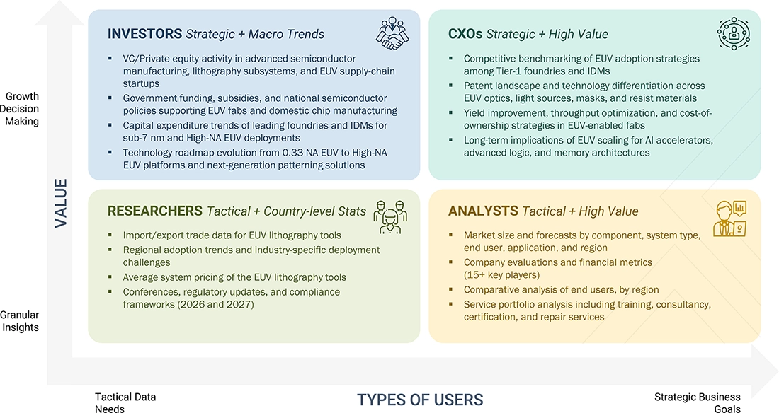
DELIVERED CUSTOMIZATIONS
We have successfully delivered the following deep-dive customizations:
| CLIENT REQUEST | CUSTOMIZATION DELIVERED | VALUE ADDS |
|---|---|---|
| EUV System Manufacturers (OEMs) |
|
|
| EUV Component Manufacturers |
|
|
| Semiconductor Foundries |
|
|
| Integrated Device Manufacturers (IDMs) |
|
|
| Investors & Corporate Strategy Teams |
|
|
RECENT DEVELOPMENTS
- October 2025 : Lasertec Corporation launched ACTIS A200HiT Series tailored for next-generation semiconductor photomask and mask-blank quality control. The introduction of this product reflects the company’s commitment to meeting growing industry demand for advanced lithography inspection, particularly driven by the shift toward EUV and high-NA processes. With this launch, Lasertec aims to strengthen its position as a leading supplier of high-precision inspection tools, enhance defect detection capabilities for photomasks/mask-blanks, and support global semiconductor manufacturers in maintaining yield and quality standards as chip feature sizes shrink and complexity increases.
- September 2025 : ZEISS Semiconductor Manufacturing Technology (SMT) launched AIMS EUV 3.0 as its next-generation aerial image measurement system, designed to support both low-NA and high-NA EUV lithography. The new platform substantially improves mask qualification productivity, delivering up to threefold higher throughput than earlier versions while maintaining high uptime, performance stability, and cost-efficient operation. Already deployed at leading semiconductor manufacturers, AIMS EUV 3.0 enables accurate mask-to-wafer imaging conditions essential for next-generation EUV lithography processes.
- July 2025 : Lasertec Corporation launched the EPM200, an advanced inspection system designed to detect and classify particles on next-generation EUV carbon nanotube pellicles. It introduces a breakthrough capability to identify whether defects are on the front or back side of the pellicle, enhancing quality control for pellicle manufacturers and device makers. The product further strengthens Lasertec’s comprehensive EUV inspection portfolio across masks, mask blanks, and pellicles.
- March 2025 : ASML and imec ntered into a multi-year strategic partnership aimed at advancing semiconductor research and driving sustainable innovation within Europe. The collaboration encompasses joint R&D initiatives, shared access to pilot production lines, and deep integration across ASML’s full technology portfolio, including 0.55 NA EUV, 0.33 NA EUV, DUV immersion, YieldStar optical metrology, and HMI single- and multi-beam technologies to accelerate technology maturation and promote more sustainable manufacturing practices.
- March 2025 : ZEISS and imec signed a renewed strategic partnership agreement extending their collaboration through 2029 to drive next-generation semiconductor research and manufacturing. Under this agreement, ZEISS will support imec’s new NanoIC pilot line, a cutting-edge facility focused on sub-2 nm technology, by supplying high-precision lithography optics (used in ASML scanners) and collaborating on advanced process development, inspection, and measurement methods. The central aim of the partnership is to advance and refine high-NA EUV lithography, enabling the production of more powerful, efficient, and compact microchips and reinforcing Europe’s competitiveness through initiatives such as the European Chips Act.
Table of Contents

Methodology
The study involved significant activities in estimating the current market size for the EUV lithography market. Exhaustive secondary research was done to collect information on the EUV lithography industry. The next step was to validate these findings, assumptions, and sizing with industry experts across the value chain using primary research. Different approaches, such as top-down and bottom-up, were employed to estimate the total market size. After that, the market breakup and data triangulation procedures were used to estimate the market size of the segments and subsegments of the EUV lithography market.
Secondary Research
The market for the companies offering EUV lithography systems and components is arrived at by secondary data available through paid and unpaid sources, analyzing the product portfolios of the major companies in the ecosystem, and rating the companies by their performance and quality. Various sources were referred to in the secondary research process to identify and collect information for this study. The secondary sources include annual reports, press releases, investor presentations of companies, white papers, journals, certified publications, and articles from recognized authors, directories, and databases. In the secondary research process, various secondary sources were referred to determine and collect information related to the scope of the study. Secondary sources included annual reports, press releases, investor presentations of EUV lithography equipment manufacturers, certified publications, and whitepapers. The secondary research was used to obtain critical information on the industry's value chain, the total pool of key players, market classification, and segmentation from the market and technology-oriented perspectives.
Primary Research
In the primary research process, various supply and demand sources were interviewed to obtain qualitative and quantitative information for this report. The primary sources from the supply side included industry experts, such as Chief Executive Officers (CEOS), Vice Presidents (VPs), marketing directors, technology and innovation directors, and related key executives from various key companies and organizations operating in the EUV lithography market.
After the complete market engineering (calculations for market statistics, market breakdown, market size estimations, market forecasting, and data triangulation), extensive primary research was conducted to gather information and verify and validate the critical numbers arrived at. Primary research was also conducted to identify the segmentation types, industry trends, competitive landscape of EUV lithography solutions offered by various market players, and key market dynamics, such as drivers, restraints, opportunities, challenges, industry trends, and key player strategies.
In the complete market engineering process, the top-down and bottom-up approaches were extensively used, along with several data triangulation methods, to perform the market estimation and market forecasting for the overall market segments and subsegments listed in this report.
Extensive qualitative and quantitative analysis was performed on the complete market engineering process to list the key information/insights throughout the report.
To know about the assumptions considered for the study, download the pdf brochure
Market Size Estimation
The market engineering process extensively employed the top-down and bottom-up approaches. Various data triangulation methods were utilized to forecast and estimate the market segments and subsegments covered in the report. Multiple qualitative and quantitative analyses were conducted during the market engineering to extract key insights throughout the report.
Secondary research helped identify key players in the EUV lithography market. Their revenues were determined through a combination of primary and secondary research, analyzed both geographically and by market segment, using financial statements and annual reports. Insights were further enriched through interviews with CEOs, VPs, directors, and marketing executives.
Market shares were estimated using this combined research approach. The data was then consolidated, supplemented with detailed inputs and analysis from MarketsandMarkets, and presented in the report.
Extreme Ultraviolet (EUV) Lithography Market : Top-Down and Bottom-Up Approach

Data Triangulation
The market was split into three segments and subsegments after arriving at the overall market size using the market size estimation processes explained above. The data triangulation and market breakup procedures were employed, wherever applicable, to complete the overall market engineering process and arrive at the exact statistics of each market segment and subsegment. The data was triangulated by studying various factors and trends from both the demand and supply sides.
Market Definition
EUV Lithography is a leading semiconductor manufacturing process, allowing to build smaller and more intricate computer chips. By using an extreme ultraviolet light of ~13.5 nanometers, facilitates making etch features on a silicon wafer, a technology that helps in minimizing the size of transistors, and allows the miniaturization of transistors and the development of intricate and detailed integrated circuits. The modern systems of EUV lithography achieve resolutions as small as 5 nanometers and aid in the production of high-performance, energy-efficient processors.
It is divided mainly into key steps, such as source generation, light collection, and conditioning. Mask fabrication, projection, imaging, photoresist application, exposure, development, etching, deposition, and iterative processing are also considered in the processing. Some of the principal components of an EUV system are found to be the light sources, optics, masks, metrology tools, sensors, and subassemblies.
Key Stakeholders
- Semiconductor Manufacturers
- EUV Lithography Component Suppliers
- Raw Material Providers
- Metrology and Inspection Equipment Providers
- Foundries and IDMs (Integrated Device Manufacturers)
- Research Institutions and Consortia
- Government Agencies and Funding Bodies
Report Objectives
The following are the primary objectives of the study.
- To define, describe, and forecast the size of the extreme ultraviolet (EUV) lithography market by component, end user, and region in terms of value.
- To describe and forecast the market size for various segments with regard to three main regions: Asia Pacific, the Americas, and Europe
- To forecast the shipments of EUV lithography systems from 2024 to 2029
- To provide detailed information regarding the key factors such as drivers, restraints, opportunities, and challenges influencing the growth of the market
- To provide macroeconomic outlooks with respect to main regions namely the Americas, Europe, and Asia Pacific
- To provide a detailed overview of the extreme ultraviolet (EUV) lithography market value chain, industry trends, technology trends, use cases, regulatory landscape, and Porter’s five forces.
- To strategically analyze micromarkets with respect to individual growth trends, prospects, and contributions to the total market
- To provide ecosystem analysis, trends/disruptions impacting customer business, technology analysis, pricing analysis, key stakeholders & buying criteria, case study analysis, trade analysis, patent analysis, key conferences & events, Gen AI/ AI impact, and regulations related to the extreme ultraviolet (EUV) lithography market
- To analyze the opportunities in the market for stakeholders by identifying high-growth segments and detailing the competitive landscape for market players.
- To strategically profile key players and comprehensively analyze their market rankings, core competencies, company valuation and financial metrics, and product/brand comparison, along with detailing the competitive landscape for the market leaders
- To analyze the competitive developments, such as product launch and collaboration carried out by market players
- To benchmark players within the market using the proprietary competitive leadership mapping framework, which analyzes market players on various parameters within the broad categories of business strategy excellence and strength of product portfolio
Available Customizations
With the given market data, MarketsandMarkets offers customizations according to the specific requirements of companies. The following customization options are available for the report:
- Country-wise information for Asia Pacific
- Detailed analysis and profiling of additional market players (up to five)
Need a Tailored Report?
Customize this report to your needs
Get 10% FREE Customization
Customize This ReportPersonalize This Research
- Triangulate with your Own Data
- Get Data as per your Format and Definition
- Gain a Deeper Dive on a Specific Application, Geography, Customer or Competitor
- Any level of Personalization
Let Us Help You
- What are the Known and Unknown Adjacencies Impacting the Extreme Ultraviolet (EUV) Lithography Market
- What will your New Revenue Sources be?
- Who will be your Top Customer; what will make them switch?
- Defend your Market Share or Win Competitors
- Get a Scorecard for Target Partners
Custom Market Research Services
We Will Customise The Research For You, In Case The Report Listed Above Does Not Meet With Your Requirements
Get 10% Free CustomisationTESTIMONIALS





Growth opportunities and latent adjacency in Extreme Ultraviolet (EUV) Lithography Market