
Advanced Process Nodes Market Size, Share & Trends
Advanced Process Nodes Market by Node Size (= 2 nm, 3 nm, 4 nm, 5 nm, 6 nm, 7 nm, = 10 nm), Packaging Technology (SiP, Flip-Chip, 2.5D/3D, WLCSP, FO), Processor Type (CPU, GPU, FPGA, ASIC, SoC), Architecture, Application, Region - Global Forecast to 2032


OVERVIEW

Source: Secondary Research, Interviews with Experts, MarketsandMarkets Analysis
The advanced process nodes market is projected to reach USD 152.55 billion by 2032 from USD 86.12 billion in 2025, at a CAGR of 8.5% from 2025 to 2032. The growth of the advanced process nodes market is driven by the escalating demand for high-performance, energy-efficient chips powering AI, 5G, and edge computing applications. Additionally, continuous investments in semiconductor fabrication technologies and the development of sub-3nm nodes will accelerate market expansion.
KEY TAKEAWAYS
-
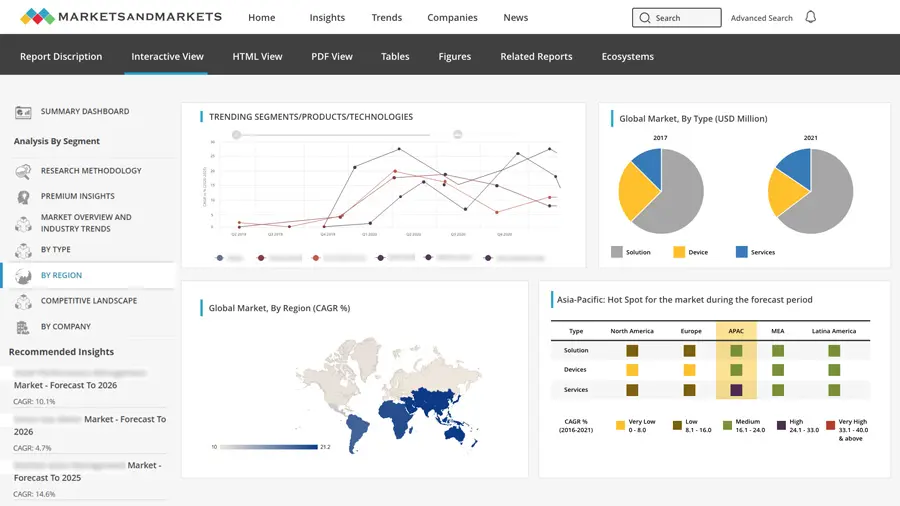
By RegionThe Asia Pacific Advanced Process Nodes market accounted for a 71.8% revenue share in 2024.
-
By Node SizeBy node size, the ≤ 2 nm segment is expected to register the highest CAGR for advanced process nodes market.
-
By Packaging TechnologyBy packaging technology, the flip-chip segment is expected to dominate the market.
-
By Processor TypeBy processor type, the GPU segment is expected to grow at the fastest rate from 2025 to 2032.
-
By ArchitectureBy architecture, the RISC-V segment will grow the fastest during the forecast period.
-
By ApplicationBy application, the data center segment is expected to dominate the market, growing at the highest CAGR during forecast period.
The Advanced Process Nodes market is experiencing robust growth, driven by surging demand for high-performance, energy-efficient chips to power next-generation applications in AI, 5G, automotive electronics, and high-performance computing. Ongoing advancements in lithography, transistor architectures, and packaging technologies are enabling smaller, faster, and more power-efficient semiconductors. Strategic collaborations between foundries, fabless players, and equipment manufacturers, along with government-backed semiconductor initiatives, are accelerating innovation and strengthening global manufacturing capacity.
TRENDS & DISRUPTIONS IMPACTING CUSTOMERS' CUSTOMERS
The Advanced Process Nodes Market is undergoing a major transformation as demand shifts from high-volume consumer products and commodity logic chips toward AI accelerators, chiplets, and advanced 2nm and sub-2nm nodes. This evolution is driven by emerging use cases in AI, HPC, and edge computing, alongside new design-technology collaborations and ecosystem partnerships. Fabless semiconductor firms, IDMs, OSATs, and AI startups are aligning with hyperscalers, automotive OEMs, and data center operators to enable next-generation performance and efficiency. The result is an ecosystem focused on AI-driven performance optimization, reduced latency, lower power consumption, and scalability for high-performance cloud and edge workloads.

Source: Secondary Research, Interviews with Experts, MarketsandMarkets Analysis
MARKET DYNAMICS
Level
-
Rising demand for AI, ML, and HPC applications

-
Proliferation of 5G networks and connected devices

Level
-
High capital expenditure and long development cycles

-
Limited availability of skilled workforce and technical expertise

Level
-
Surge in data center and cloud infrastructure expansion

-
Integration of AI and automation in chip design and fabrication

Level
-
Complex design verification and validation

-
Material and lithography limitations

Source: Secondary Research, Interviews with Experts, MarketsandMarkets Analysis
Driver: Rising demand for AI, ML, and HPC applications
The growing adoption of artificial intelligence, machine learning, and high-performance computing workloads is fueling the demand for chips built on advanced process nodes. These applications require exceptional processing power, low latency, and high energy efficiency, which are the capabilities that smaller geometries like 5nm and 3nm can deliver.
Restraint: High capital expenditure and long development cycles
Developing and manufacturing chips at sub-7nm process nodes requires massive investments in R&D, fabrication facilities, and EUV lithography equipment. The cost of building a leading-edge fab now exceeds tens of billions of dollars, creating entry barriers for new players and limiting innovation to a few dominant foundries.
Opportunity: Surge in data center and cloud infrastructure expansion
The rapid expansion of hyperscale data centers and cloud computing environments is driving significant demand for advanced processors and memory built on cutting-edge nodes. As cloud providers prioritize performance, energy efficiency, and workload scalability, advanced process technologies enable more powerful and compact chips to support AI inference, virtualization, and analytics.
Challenge: Complex design verification and validation
At advanced process nodes, verifying and validating chip designs becomes increasingly difficult due to extreme miniaturization, higher transistor counts, and signal integrity issues. Ensuring functional accuracy, reliability, and manufacturability across billions of transistors demands sophisticated EDA tools, extensive simulation, and iterative testing.
advanced-process-nodes-market: COMMERCIAL USE CASES ACROSS INDUSTRIES
| COMPANY | USE CASE DESCRIPTION | BENEFITS |
|---|---|---|
 |
Integrated AMD’s Zynq UltraScale+ MPSoC into next-generation TRACE32 debugging tools to enhance performance, flexibility, and compatibility across 150+ chip architectures. | Achieved faster response times and lower latency through task-level optimization; enabled 80 Gb/s trace bandwidth and improved debugging efficiency and power management. |
|
|
Developed Eyeonic vision sensors using AMD’s Zynq UltraScale+ RFSoC, integrating RF-sampling ADCs and DACs to support advanced FMCW LiDAR functions. | Delivered sub-millimeter precision and extended LiDAR range; reduced power consumption and footprint; achieved flexible, scalable, and energy-efficient architecture for future innovations. |
|
|
Adopted AMD’s Zynq-7000S SoC to modernize the TBS1000 oscilloscope series for educational and entry-level markets, ensuring long-term durability and cost-effectiveness. | Achieved 8× increase in record length and 10× faster waveform capture; enhanced software features, user interface, and time-to-market efficiency with reduced production cost. |
 |
Partnered with Intel Corporation to deploy Cyclone IV FPGAs in SMT production lines for real-time processing and Industry 4.0 integration. | Improved efficiency, reduced downtime, and enabled predictive maintenance with enhanced data analytics and connectivity. |
|
|
Used AMD Artix UltraScale+ FPGAs for next-gen 4K capture devices supporting 20 Gb/s USB 3.2 Gen 2x2 connectivity. | Achieved faster data transfer, lower power use, simpler design, and faster time-to-market with superior video quality. |
Logos and trademarks shown above are the property of their respective owners. Their use here is for informational and illustrative purposes only.
MARKET ECOSYSTEM
The advanced process nodes market ecosystem comprises a highly interconnected network of material suppliers, semiconductor foundries, fabless chip designers, and system integrators. Material providers enable wafer quality and purity essential for next-generation nodes, while foundries drive process innovation and high-volume manufacturing. Fabless chip designers leverage these advanced nodes to create high-performance, energy-efficient processors, and system integrators incorporate them into cutting-edge devices across electronics, automotive, and data center applications.

Logos and trademarks shown above are the property of their respective owners. Their use here is for informational and illustrative purposes only.
MARKET SEGMENTS

Source: Secondary Research, Interviews with Experts, MarketsandMarkets Analysis
Advanced Process Nodes Market, By Node Size
As of 2024, 5nm technology dominated the advanced process nodes market, supported by large-scale deployment in flagship smartphones, high-performance computing chips, and data center processors. Leading foundries such as TSMC, Samsung, and Intel have achieved strong yield maturity at 5nm, enabling high transistor density, better energy efficiency, and improved performance per watt. With ongoing optimization and design ecosystem maturity, the 5nm node continues to serve as a critical inflection point bridging mass-market affordability with advanced AI and HPC performance requirements.
Advanced Process Nodes Market, By Packaging Technology
In 2024, Flip-Chip packaging held a significant share of the advanced process nodes market, driven by its superior electrical performance, thermal efficiency, and scalability for high I/O density devices. Flip-Chip Chip Scale Packages (FCCSP) and Flip-Chip Ball Grid Arrays (FCBGA) are widely adopted in CPUs, GPUs, and SoCs due to their ability to handle higher power and speed requirements at advanced geometries. With its established manufacturing base and compatibility with high-volume production, Flip-Chip remains a cornerstone packaging solution for performance-intensive semiconductor applications.
Advanced Process Nodes Market, By Processor Type
The GPU segment accounted for the largest share of the advanced process nodes market in 2024, propelled by explosive growth in AI training, deep learning, and data analytics workloads. Modern GPUs, manufactured at 5nm and below, deliver exceptional parallel processing capability, power efficiency, and memory bandwidth, making them indispensable for data centers and edge AI systems. Major players such as NVIDIA, AMD, and Intel continue to migrate their GPU architectures to smaller nodes, further enhancing performance-per-watt and driving market expansion.
Advanced Process Nodes Market, By Architecture
In 2024, the ARM architecture segment dominated the advanced process nodes market, fueled by its widespread adoption across mobile devices, IoT systems, and emerging data center applications. ARM’s power-efficient design and scalability make it a preferred choice for SoCs built on 5nm and 3nm nodes, particularly for AI and edge computing workloads. As hyperscalers and semiconductor firms increasingly adopt custom ARM-based designs, the architecture’s ecosystem continues to expand, reinforcing its leadership in the post-x86 era of compute innovation.
Advanced Process Nodes Market, By Application
The data center segment is expected to dominate the advanced process nodes market and witness the highest growth rate through 2033, driven by exponential increases in AI model training, cloud computing, and virtualization workloads. Advanced nodes such as 5nm, 3nm, and emerging 2nm enable processors with superior performance, energy efficiency, and density—critical for managing high-throughput, low-latency operations in hyperscale environments. With major cloud providers and chipmakers investing heavily in next-generation server architectures, data centers will remain a primary growth engine for advanced process technologies.
REGION
Asia Pacific to be fastest-growing region in global advanced process nodes market during forecast period
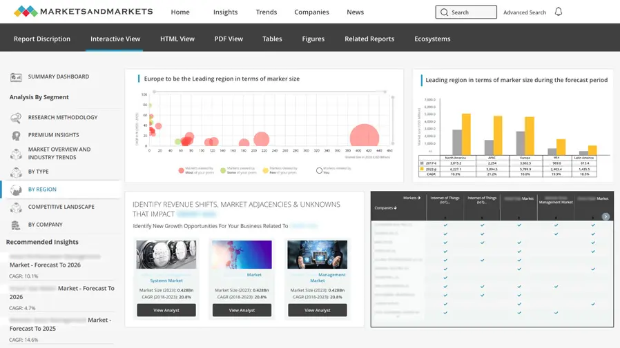
The Asia Pacific region is expected to register the highest CAGR in the Advanced Process Nodes Market during the forecast period, driven by rapid expansion of semiconductor manufacturing capacity and strong government support across key economies such as Taiwan, South Korea, China, and Japan. The region hosts leading foundries including TSMC, Samsung Electronics, and SMIC, which are heavily investing in sub-5nm and 3nm technologies to meet surging global demand for AI, 5G, and high-performance computing applications. Additionally, rising adoption of advanced chips in consumer electronics, automotive electronics, and data centers, coupled with government-backed initiatives like Japan’s semiconductor revitalization program and India’s Semiconductor Mission, is fostering a robust ecosystem for R&D and fabrication.

advanced-process-nodes-market: COMPANY EVALUATION MATRIX
In the advanced process nodes market matrix, TSMC (Star) leads with a commanding market share and a robust technology portfolio, driven by its early commercialization of 5nm and 3nm nodes and strong partnerships across AI, HPC, and mobile segments. The company’s extensive foundry capacity, advanced EUV lithography adoption, and continuous R&D investment position it at the forefront of semiconductor innovation and process scalability. GlobalFoundries (Emerging Leader) is gaining prominence through its focus on specialized, power-efficient nodes and strategic collaborations targeting automotive, IoT, and industrial applications.

Source: Secondary Research, Interviews with Experts, MarketsandMarkets Analysis
KEY MARKET PLAYERS
MARKET SCOPE
| REPORT METRIC | DETAILS |
|---|---|
| Market Size in 2024 (Value) | USD 76.63 Billion |
| Market Forecast in 2030 (Value) | USD 152.55 Billion |
| Growth Rate | CAGR of 8.5% from 2025-2032 |
| Years Considered | 2021-2032 |
| Base Year | 2024 |
| Forecast Period | 2025-2032 |
| Units Considered | Value (USD Billion) |
| Report Coverage | Revenue forecast, company ranking, competitive landscape, growth factors, and trends |
| Segments Covered |
|
| Regions Covered | North America, Europe, Asia Pacific, RoW |
WHAT IS IN IT FOR YOU: advanced-process-nodes-market REPORT CONTENT GUIDE

DELIVERED CUSTOMIZATIONS
We have successfully delivered the following deep-dive customizations:
| CLIENT REQUEST | CUSTOMIZATION DELIVERED | VALUE ADDS |
|---|---|---|
| Leading Chip Designer / IDM |
|
|
| Semiconductor Foundry |
|
|
| Packaging & OSAT Provider |
|
|
| EDA / Design Automation Firm |
|
|
| Consumer Electronics / Automotive OEM |
|
|
RECENT DEVELOPMENTS
- April 2025 : TSMC announced its next-generation A14 logic process technology at the North America Technology Symposium, marking a major leap beyond its 2nm (N2) node. Designed to accelerate AI transformation and enhance power efficiency, A14 delivers up to 15% higher speed or 30% lower power and a 20% increase in logic density compared to N2.
- April 2025 : Advanced Micro Devices, Inc. launched its next-generation EPYC processor, codenamed “Venice,” developed on TSMC’s advanced 2nm (N2) process technology. This reinforces the strong AMD–TSMC collaboration in co-optimizing cutting-edge architectures and manufacturing innovation. “Venice” marks a major advancement in AMD’s data center CPU roadmap, alongside the successful validation of AMD’s 5th Gen EPYC CPUs at TSMC’s new Arizona fab, emphasizing AMD’s commitment to US-based semiconductor production.
- June 2024 : Samsung Electronics introduced two new advanced process nodes, SF2Z and SF4U, alongside its integrated Samsung AI Solutions platform, combining Foundry, Memory, and Advanced Packaging capabilities to meet accelerating AI demand. The new SF2Z 2nm process features a backside power delivery network (BSPDN) that improves power, performance, and area efficiency while reducing voltage drop, optimizing it for high-performance computing and AI workloads.
Table of Contents
 Exclusive indicates content/data unique to MarketsandMarkets and not available with any competitors.
- 5.1 INTRODUCTION
-
5.2 PORTERS FIVE FORCE ANALYSISTHREAT FROM NEW ENTRANTSTHREAT OF SUBSTITUTESBARGAINING POWER OF SUPPLIERSBARGAINING POWER OF BUYERSINTENSITY OF COMPETITIVE RIVALRY
-
5.3 MACROECONOMICS INDICATORSINTRODUCTIONGDP TRENDS AND FORECASTTRENDS IN GLOBAL LOGIC SEMICONDUCTOR INDUSTRY
- 5.4 VALUE CHAIN ANALYSIS
- 5.5 ECOSYSTEM ANALYSIS
-
5.6 PRICING ANALYSISAVERAGE SELLING PRICE OF KEY PLAYERS, BY NODE SIZE, 2024AVERAGE SELLING PRICE, BY PROCESSOR TYPE, 2021–2024AVERAGE SELLING PRICE, BY ARCHITECTURE, 2021–2024AVERAGE SELLING PRICE, BY REGION, 2021–2024
-
5.7 TRADE ANALYSISIMPORT SCENARIOEXPORT SCENARIO
- 5.8 KEY CONFERENCES AND EVENTS, 2025–2026
- 5.9 TRENDS/DISRUPTIONS IMPACTING CUSTOMER BUSINESS
- 5.10 INVESTMENT AND FUNDING SCENARIO
- 5.11 CASE STUDY ANALYSIS
-
5.12 IMPACT OF 2025 US TARIFF – ADVANCED PROCESS NODES MARKETINTRODUCTIONKEY TARIFF RATESPRICE IMPACT ANALYSISIMPACT ON COUNTRIES/REGIONSIMPACT ON VERTICALS
- 6.1 KEY EMERGING TECHNOLOGIES
- 6.2 COMPLEMENTARY TECHNOLOGIES
- 6.3 TECHNOLOGY/PRODUCT ROADMAP
- 6.4 PATENT ANALYSIS
- 6.5 FUTURE APPLICATIONS
- 6.6 IMPACT OF AI/GEN AI ON ADVANCED PROCESS NODES MARKET
- 6.7 TOP USE CASES AND MARKET POTENTIAL
- 6.8 BEST PRACTICES IN ADVANCED PROCESS NODES
- 6.9 CASE STUDIES OF AI IMPLEMENTATION IN THE ADVANCED PROCESS NODES MARKET
- 6.10 INTERCONNECTED ADJACENT ECOSYSTEM AND IMPACT ON MARKET PLAYERS
- 6.11 CLIENTS’ READINESS TO ADOPT GENERATIVE AI IN ADVANCED PROCESS NODES MARKET
- 6.12 SUCCESS STORIES AND REAL-WORLD APPLICATIONS
-
7.1 REGIONAL REGULATIONS AND COMPLIANCEREGULATORY BODIES, GOVERNMENT AGENCIES, AND OTHER ORGANIZATIONSINDUSTRY STANDARDS
-
7.2 SUSTAINABILITY INITIATIVESCARBON IMPACT AND ECO-APPLICATIONS OF ADVANCED PROCESS NODES
- 7.3 SUSTAINABILITY IMPACT AND REGULATORY POLICY INITIATIVES
- 7.4 CERTIFICATIONS, LABELING, ECO-STANDARDS
- 8.1 DECISION-MAKING PROCESS
- 8.2 BUYER STAKEHOLDERS AND BUYING EVALUATION CRITERIA
- 8.3 ADOPTION BARRIERS & INTERNAL CHALLENGES
- 8.4 UNMET NEEDS FROM VARIOUS VERTICALS
- 8.5 MARKET PROFITABILITY
- 9.1 INTRODUCTION
- 9.2 ≤ 2 NM
- 9.3 3 NM
- 9.4 4 NM
- 9.5 5 NM
- 9.6 6 NM
- 9.7 7 NM
- 9.8 ≥ 10 NM
- 10.1 INTRODUCTION
- 10.2 SYSTEM-IN-PACKAGE (SIP)
-
10.3 FLIP-CHIPFLIP-CHIP CHIP SCALE PACKAGE (FCCSP)FLIP-CHIP BALL GRID ARRAY (FCBGA)
- 10.4 2.5D/3D
- 10.5 WAFER-LEVEL CHIP SCALE PACKAGE (WLCSP)
- 10.6 FAN-OUT (FO)
- 11.1 INTRODUCTION
- 11.2 CPU
- 11.3 GPU
- 11.4 FPGA
- 11.5 ASIC
- 11.6 SOC/ APPLICATION PROCESSORS
- 12.1 INTRODUCTION
- 12.2 ARM
- 12.3 X86
- 12.4 RISC-V
- 12.5 OTHERS
- 13.1 INTRODUCTION
-
13.2 CONSUMER ELECTRONICSSMARTPHONESAI PCSTABLETLAPTOPWEARABLESOTHERS
-
13.3 DATA CENTERSERVERS- GPU Servers- FPGA Servers- ASIC ServersINTERCONNECTSHIGH-SPEED SWITCHES & ROUTERSSTORAGE CONTROLLERS / SSD CONTROLLERS
- 13.4 HIGH-PERFORMANCE COMPUTING (HPC)
-
13.5 AUTOMOTIVEADAS & AUTONOMOUS DRIVING- ADAS SoCs- Radar signal processors- LiDAR processing units- Sensor fusion processors- Domain controllersINFOTAINMENT & CONNECTIVITYELECTRIC VEHICLES (EVS)
-
13.6 NETWORKING & TELECOMMUNICATIONS5G / 6G INFRASTRUCTUREEDGE COMPUTING DEVICESNETWORKING EQUIPMENT
-
13.7 INDUSTRIALVIDEO SURVEILLANCE SYSTEMSMACHINE VISION SOLUTIONSINDUSTRIAL NETWORKING SOLUTIONSINDUSTRIAL MOTOR CONTROL SOLUTIONSROBOTICSINDUSTRIAL SENSORSOTHERS
-
13.8 DEFENSE & AEROSPACERADAR AND SIGNAL PROCESSING SYSTEMSSATELLITE COMMUNICATION PROCESSORSSECURE COMMUNICATION ASICSUAV/DRONE COMPUTE MODULESHIGH-RELIABILITY EMBEDDED PROCESSORS
- 13.9 OTHER APPLICATIONS
- 14.1 INTRODUCTION
-
14.2 NORTH AMERICAUSCANADAMEXICO
-
14.3 EUROPEGERMANYUKFRANCEITALYNORDICSREST OF EUROPE
-
14.4 ASIA PACIFICCHINAJAPANSOUTH KOREATAIWANREST OF ASIA PACIFIC
- 14.5 REST OF THE WORLD
- 15.1 OVERVIEW
- 15.2 KEY PLAYER STRATEGIES/RIGHT TO WIN
- 15.3 REVENUE ANALYSIS, 2021-2024
- 15.4 MARKET SHARE ANALYSIS, 2024
- 15.5 BRAND/PRODUCT COMPARISON
-
15.6 COMPANY EVALUATION MATRIX: KEY PLAYERS, 2024STARSEMERGING LEADERSPERVASIVE PLAYERSPARTICIPANTSCOMPANY FOOTPRINT: KEY PLAYERS, 2024- Company Footprint- Region Footprint- Node Size Footprint- Packaging Technology Footprint- Application Footprint
-
15.7 COMPANY EVALUATION MATRIX: STARTUPS/SMES, 2024PROGRESSIVE COMPANIESRESPONSIVE COMPANIESDYNAMIC COMPANIESSTARTING BLOCKSCOMPETITIVE BENCHMARKING: STARTUPS/SMES, 2024- Detailed List of Key Startups/SMEs- Competitive Benchmarking of Key Startups/SMEs
- 15.8 COMPANY VALUATION AND FINANCIAL METRICS
-
15.9 COMPETITIVE SCENARIOPRODUCT LAUNCHESDEALSEXPANSIONS
-
16.1 KEY PLAYERSTAIWAN SEMICONDUCTOR MANUFACTURING COMPANY LIMITED (TSMC)SAMSUNG ELECTRONICS CO., LTD.INTEL CORPORATIONSEMICONDUCTOR MANUFACTURING INTERNATIONAL CORPORATION (SMIC)GLOBALFOUNDRIES INC.UNITED MICROELECTRONICS CORPORATION (UMC)TOWER SEMICONDUCTOR LTD.POWERCHIP SEMICONDUCTOR MANUFACTURING CORPORATION (PSMC)VANGUARD INTERNATIONAL SEMICONDUCTOR CORPORATION (VIS)SHANGHAI HUA HONG INTEGRATED CIRCUIT CO., LTD.
-
16.2 OTHER PLAYERSDB HITEK CO., LTD.X-FAB SILICON FOUNDRIES SESILTERRA MALAYSIA SDN. BHD.SHANGHAI HUAHONG GRACE SEMICONDUCTOR MANUFACTURING CORPORATIONSTMICROELECTRONICS N.V.TEXAS INSTRUMENTS INCORPORATEDINFINEON TECHNOLOGIES AGON SEMICONDUCTOR CORPORATIONNUVOTON TECHNOLOGY CORPORATIONRENESAS ELECTRONICS CORPORATION
-
17.1 RESEARCH DATASECONDARY DATA- Key Data from Secondary SourcesPRIMARY DATA- Key data from primary sources- Key primary participants- Breakdown of primary interviews- Key industry insights
-
17.2 MARKET SIZE ESTIMATIONBOTTOM-UP APPROACHTOP-DOWN APPROACHBASE NUMBER CALCULATION
-
17.3 MARKET FORECAST APPROACHSUPPLY SIDEDEMAND SIDE
- 17.4 DATA TRIANGULATION
- 17.5 FACTOR ANALYSIS
- 17.6 RESEARCH ASSUMPTIONS
- 17.7 RESEARCH LIMITATIONS AND RISK ASSESSMENT
- 18.1 DISCUSSION GUIDE
- 18.2 KNOWLEDGE STORE: MARKETSANDMARKETS’ SUBSCRIPTION PORTAL
- 18.3 CUSTOMIZATION OPTIONS
- 18.4 RELATED REPORTS
- 18.5 AUTHOR DETAILS
Need a Tailored Report?
Customize this report to your needs
Get 10% FREE Customization
Customize This ReportPersonalize This Research
- Triangulate with your Own Data
- Get Data as per your Format and Definition
- Gain a Deeper Dive on a Specific Application, Geography, Customer or Competitor
- Any level of Personalization
Let Us Help You
- What are the Known and Unknown Adjacencies Impacting the Advanced Process Nodes Market
- What will your New Revenue Sources be?
- Who will be your Top Customer; what will make them switch?
- Defend your Market Share or Win Competitors
- Get a Scorecard for Target Partners

Custom Market Research Services
We Will Customise The Research For You, In Case The Report Listed Above Does Not Meet With Your Requirements
Get 10% Free CustomisationTESTIMONIALS

Tetsuya Ohhira
Business Development Manager-Technology Business
Nikon Corporation,
Leading Japanese MNC specializing in optics and imaging productswww.nikon.com
MarketsandMarkets™ response
is quick. Their attitude is flexible and positive. Analyst Insights are globally considered and
significant. Client Services quickly respond to our inquiry and demand. Their wide range of global
surveys help us make our strategic plan.
We hope Knowledge Store will be easier to search
for a report.
VP - Marketing & Business Development
Leading Provider of Process Control Solutions
We engaged with MarketsandMarkets on a study to perform an analysis and recommend a Go-To-Market strategy for metrology and process control in the semiconductor market. The study was tailored to our targets and needs with well-defined milestones. Our overall experience with the MarketsandMarkets team was very good throughout the project in all aspects including the analysis methodologies used, the quality and depth of primary and secondary data sets, the professionalism and flexibility of the team and the ability to meet the target schedule and milestones. We want to thank MarketsandMarkets team for a job well done.


Growth opportunities and latent adjacency in Advanced Process Nodes Market