
MEMS Packaging Substrates Market Size, Share & Trends

MEMS Packaging Substrates Market by Substrate Type (Glass, Ceramic, Organic, Silicon), Application (Sensor, Actuator), Vertical (Consumer Electronics, Automotive, Industrial, Healthcare, Defense, Aerospace) and Region - Global Forecast to 2030


OVERVIEW
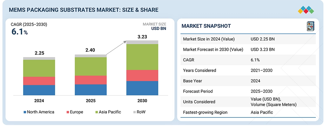
The MEMS packaging substrates market is expected to reach USD 3.23 billion by 2030, up from USD 2.40 billion in 2025, with a CAGR of 6.1% during this period. The growth is fueled by rising demand for miniaturization, enhanced thermal performance, and wafer-level packaging solutions.
Market Size & Forecast
• 2025 Market Size: USD 2.40 Billion
• 2030 Projected Market Size: USD 3.23 Billion
• CAGR (2025-2030): 6.1%
• Sensor Applications: Largest Market Share
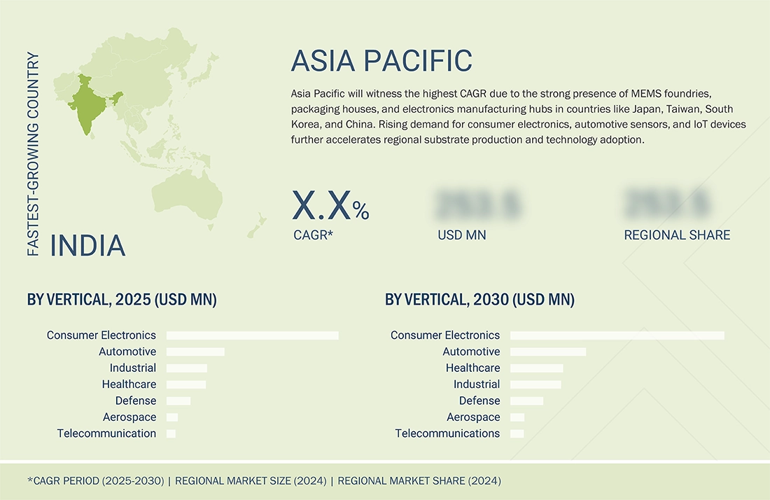
• Asia Pacific: Fastest-growing Market
KEY TAKEAWAYS
-
BY SUBSTRATE TYPESilicon substrates dominate the market because of their excellent compatibility with MEMS fabrication, high mechanical stability, and cost-effective scalability for mass production.
-
BY APPLICATIONSensor applications hold the largest market share because MEMS sensors are extensively integrated into automotive, consumer, and industrial devices, fueling high-volume demand for reliable and compact packaging solutions.
-
BY VERTICALThe telecommunications segment is expanding rapidly due to the rising adoption of MEMS-based RF components and optical sensors in 5G infrastructure and high-speed communication systems.
-
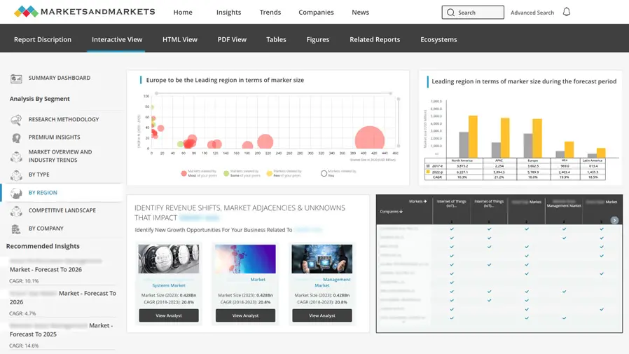
BY REGIONThe MEMS packaging substrates market covers Europe, North America, Asia Pacific, and RoW. Among these regions, Asia Pacific will grow at the highest rate due to rapid electronics manufacturing expansion, strong semiconductor supply chain presence, and rising adoption of MEMS devices in China, Japan, and South Korea.
-
COMPETITIVE LANDSCAPEMajor market participants have employed both organic and inorganic strategies, encompassing collaborations and investments. For example, CoorsTek Inc. (United States), KYOCERA Corporation (Japan), and AGC Inc. (Japan) have entered into numerous agreements and partnerships to address the increasing demand for MEMS packaging substrates across innovative applications.
The growth of the MEMS packaging substrates industry is driven by increasing use of MEMS sensors and actuators in automotive, consumer electronics, industrial automation, and healthcare sectors. Advances in materials like alumina, aluminum nitride, silicon, and glass, along with the development of Through-Glass Via (TGV) and wafer-level bonding technologies, are improving performance and increasing integration density. Moreover, the rise of IoT devices, smart wearables, and autonomous systems is boosting demand for durable, miniature MEMS packaging substrates.
Source: Secondary Research, Interviews with Experts, MarketsandMarkets Analysis
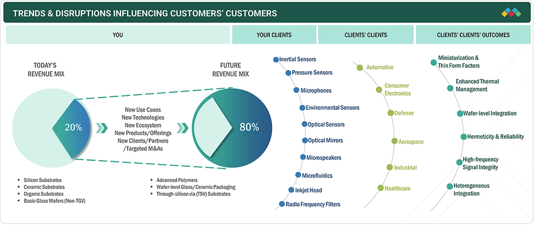
TRENDS & DISRUPTIONS IMPACTING CUSTOMERS' CUSTOMERS
The MEMS packaging substrate ecosystem is going through a major shift driven by emerging technologies and changing end-user demands. While traditional materials like silicon, ceramic, and organic substrates have long dominated the market, the future revenue composition is increasingly moving toward new sources such as advanced polymers, wafer-level glass or ceramic packaging, and through-silicon via (TSV) substrates. These innovations are supporting the development of advanced MEMS applications like inertial, pressure, and environmental sensors, optical components, microfluidics, and RF filters.
Source: Secondary Research, Interviews with Experts, MarketsandMarkets Analysis
MARKET DYNAMICS
Level
-
Rising MEMS Sensor Adoption in IoT & Consumer Devices

-
Increasing miniaturization and High-Density Integration

Level
-
High Cost of Advanced Materials and Processes

-
Complexity of Integration

Level
-
Medical & Healthcare Devices Expansion

-
Opportunities in 5G and IoT Deployment

Level
-
Thermal & Electrical Management at Small Nodes

-
Supply Chain Dependence

Source: Secondary Research, Interviews with Experts, MarketsandMarkets Analysis
Driver: Rising MEMS Sensor Adoption in IoT & Consumer Devices
The increasing demand for smart devices, wearables, and IoT applications is boosting MEMS sensor adoption. These sensors deliver accurate motion, pressure, and environmental data, enabling advanced features in smartphones, fitness trackers, smart home gadgets, and automotive systems. As consumer electronics and connected devices grow rapidly, manufacturers are increasingly depending on MEMS packaging substrates for miniaturization, enhanced performance, and reliability, fueling substantial growth in the MEMS packaging substrates market.
Restraint: High Cost of Advanced Materials and Processes
MEMS packaging substrates often require advanced materials such as silicon, ceramics, or specialized glass, along with sophisticated fabrication processes including precision lithography, wafer bonding, and through-silicon vias. These high-cost materials and complex processes increase production expenses, affecting the overall affordability of MEMS devices. Small-scale manufacturers may find it difficult to adopt these substrates, limiting market penetration. High production costs also put pricing pressure on end products, slowing adoption in price-sensitive segments like consumer electronics.
Opportunity: Medical & Healthcare Devices Expansion
The healthcare and medical device sector is increasingly adopting MEMS sensors for applications such as implantable devices, diagnostic tools, wearable health monitors, and lab-on-chip systems. MEMS packaging substrates are essential for miniaturization, biocompatibility, and ensuring reliable sensor performance in these devices. The rising focus on remote health monitoring, telemedicine, and personalized healthcare offers a lucrative market opportunity, as demand for compact, accurate, and high-performance MEMS devices is expected to grow significantly in the coming years.
Challenge: Thermal & Electrical Management at Small Nodes
As MEMS devices continue to decrease in size, effective management of heat dissipation and electrical interference becomes progressively more challenging. Miniaturized nodes produce concentrated heat and encounter signal integrity issues, which may compromise sensor performance and reliability. MEMS packaging substrates must proficiently address thermal conductivity, electrical insulation, and mechanical stability at micro- and nano-scale dimensions. Developing substrates capable of sustaining performance within these constraints presents significant technical challenges, thereby elevating R&D expenses and potentially impeding the advancement of high-performance, miniaturized MEMS devices.
MEMS Packaging Substrates Market: COMMERCIAL USE CASES ACROSS INDUSTRIES
| COMPANY | USE CASE DESCRIPTION | BENEFITS |
|---|---|---|
 |
Ceramic and glass-ceramic substrates used in automotive MEMS pressure sensors, accelerometers, and gyroscopes for advanced driver-assistance systems (ADAS) and electric vehicles | Enables high reliability under thermal and mechanical stress, supports miniaturization, and ensures long-term stability for safety-critical automotive applications |
 |
Alumina and AlN substrates supporting MEMS-based flow, pressure, and vibration sensors in industrial automation and aerospace systems | Offers superior heat dissipation, electrical insulation, and mechanical durability, extending device lifespan in extreme conditions |
 |
Ceramic packaging substrates for MEMS sensors used in medical diagnostics equipment and laboratory instrumentation | Provides biocompatibility, chemical resistance, and precision sealing for reliable sensor performance in sterile and high-sensitivity environments |
 |
Glass substrates and Through-Glass Via (TGV) wafers integrated into MEMS optical sensors and LiDAR modules for consumer electronics and autonomous vehicles | Ensures optical clarity, flatness, and fine-pitch interconnects, improving signal quality and accuracy in imaging and depth-sensing applications |
 |
Specialty glass substrates (BOROFLOAT®, FLEXINITY®) used in MEMS microphones and environmental sensors for smartphones and wearables | Provides miniaturization capability, excellent dimensional stability, and acoustic transparency, enhancing performance and device slimness |
Logos and trademarks shown above are the property of their respective owners. Their use here is for informational and illustrative purposes only.
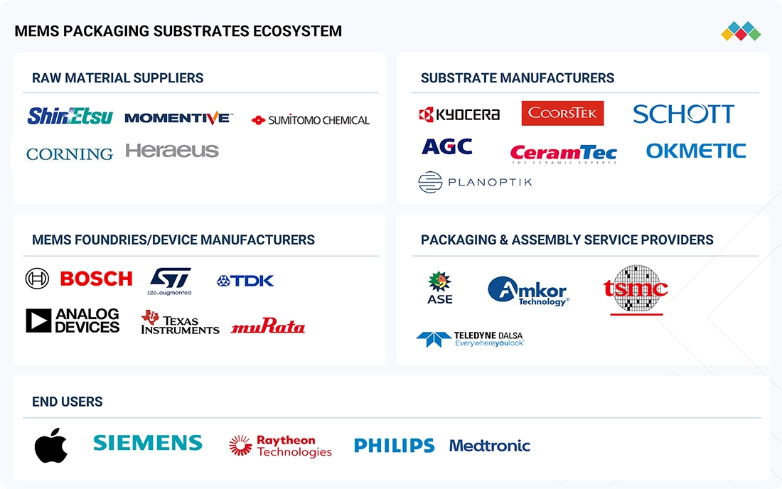
MARKET ECOSYSTEM
The MEMS packaging substrates ecosystem spans material suppliers (silicon, ceramics, glass, organics), substrate manufacturers, MEMS foundries (sensor and actuator integration), packaging/assembly providers (WLP, hermetic sealing, interconnects), and end-use industries (automotive, consumer electronics, healthcare, industrial, aerospace). Each component ensures high-performance, reliable, and miniaturized MEMS devices for diverse applications.
Logos and trademarks shown above are the property of their respective owners. Their use here is for informational and illustrative purposes only.
MARKET SEGMENTS
Source: Secondary Research, Interviews with Experts, MarketsandMarkets Analysis
MEMS Packaging Substrates Market, By Substrate Type
In the MEMS packaging substrates market, silicon holds the largest share due to its superior mechanical strength, thermal stability, and compatibility with semiconductor fabrication techniques. Its ability to support wafer-level bonding, precise micromachining, and integration with CMOS circuits makes it ideal for high-performance MEMS devices. Mature supply chains and cost efficiency at scale further reinforce silicon’s dominance in MEMS packaging substrates.
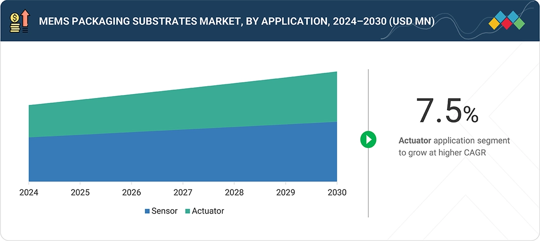
MEMS Packaging Substrates Market, By Application
In the MEMS packaging substrates market, sensor applications hold the largest share because MEMS sensors are integral to a wide range of industries, including consumer electronics, automotive, healthcare, and industrial automation. Substrates provide the mechanical stability, thermal management, and electrical insulation required for high-performance sensors like accelerometers, gyroscopes, pressure sensors, and microphones. The explosive growth of IoT devices, wearables, smartphones, and smart home products has significantly increased demand for reliable, miniaturized MEMS sensors, driving substrate adoption and making sensors the dominant application segment.
MEMS Packaging Substrates Market, By Vertical
Within the MEMS packaging substrates market, consumer electronics account for the highest demand. Smartphones, wearables, tablets, and other smart devices integrate MEMS sensors for motion tracking, orientation detection, and environmental monitoring. The need for compact, high-performance, multi-functional devices accelerates substrate adoption, making consumer electronics the primary end-use vertical driving growth in the MEMS packaging substrates market.
REGION
Asia Pacific to be fastest-growing region in global MEMS packaging substrates market during forecast period
The Asia Pacific region leads the MEMS packaging substrates market owing to its robust manufacturing infrastructure, numerous semiconductor fabrication facilities, and the presence of prominent substrate and MEMS manufacturing companies. Nations such as China, Japan, South Korea, and Taiwan benefit from extensive electronics production, particularly in consumer electronics, automotive, and Internet of Things (IoT) devices. Factors such as low production costs, government backing for cutting-edge technology, and swift adoption of smart devices further stimulate demand for MEMS substrates, establishing it as the largest and most rapidly expanding regional market within the MEMS packaging substrates sector.
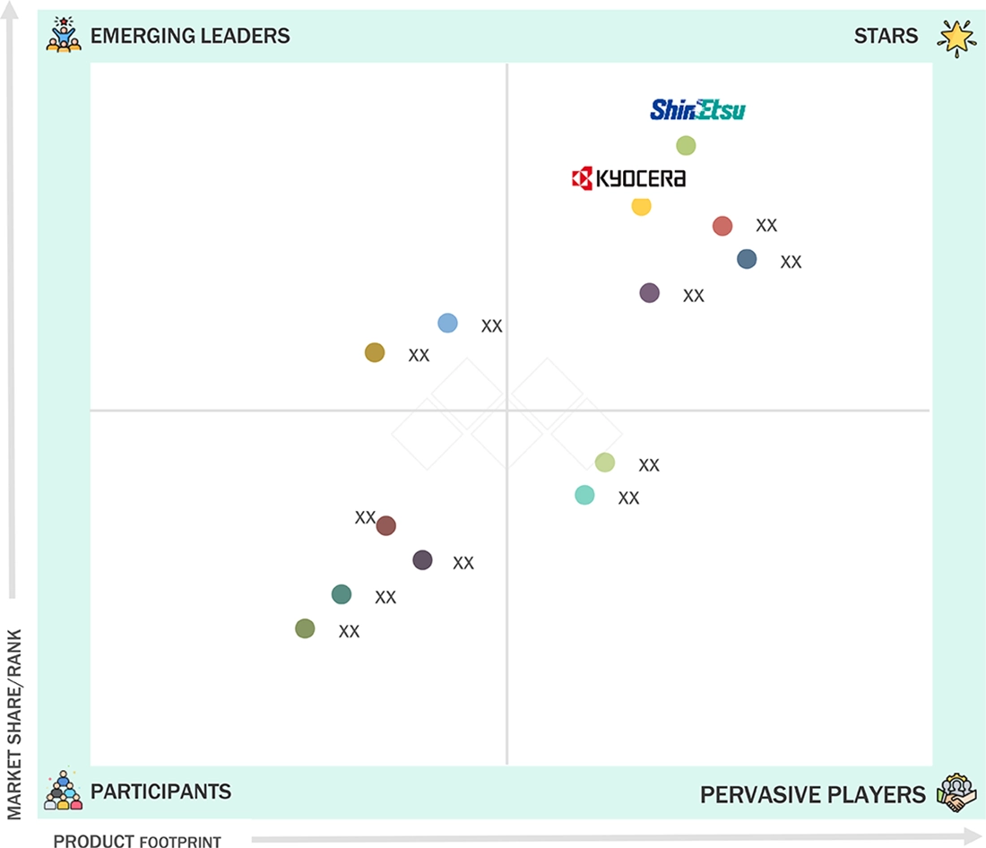
MEMS Packaging Substrates Market: COMPANY EVALUATION MATRIX
In the MEMS packaging substrates companies matrix, Shin-Etsu Chemical (Star) leads with a commanding share and broad material portfolio, driven by its high-purity silicon wafers and glass and organic substrates that enable superior reliability and performance in MEMS sensors and actuators. KYOCERA Corporation (Star) follows closely, leveraging its expertise in ceramic and glass-ceramic substrates, offering exceptional thermal stability, hermeticity, and electrical insulation.
Source: Secondary Research, Interviews with Experts, MarketsandMarkets Analysis
KEY MARKET PLAYERS
MARKET SCOPE
| REPORT METRIC | DETAILS |
|---|---|
| Market Size in 2024 (Value) | USD 2.25 Billion |
| Market Forecast in 2030 (Value) | USD 3.23 Billion |
| Growth Rate | CAGR of 6.1% from 2025-2030 |
| Years Considered | 2021-2030 |
| Base Year | 2024 |
| Forecast Period | 2025-2030 |
| Units Considered | Value (USD Million/Billion), Volume (Square Meter) |
| Report Coverage | Revenue forecast, company ranking, competitive landscape, growth factors, and trends |
| Segments Covered |
|
| Regions Covered | North America, Asia Pacific, Europe, RoW |
WHAT IS IN IT FOR YOU: MEMS Packaging Substrates Market REPORT CONTENT GUIDE
DELIVERED CUSTOMIZATIONS
We have successfully delivered the following deep-dive customizations:
| CLIENT REQUEST | CUSTOMIZATION DELIVERED | VALUE ADDS |
|---|---|---|
| MEMS Sensor Manufacturer | Competitive profiling of MEMS substrate suppliers (pricing, material types, certifications) | Benchmarking substrate usage across sensor types (accelerometers, gyros, pressure, microphones) |
| Substrate & Wafer Manufacturer | Market share analysis for silicon, glass, ceramic, and organic substrates | Comparative study of fabrication processes, yield rates, and thermal/electrical performance |
| Consumer Electronics OEM | Adoption analysis of MEMS substrates in smartphones, wearables, tablets, and smart home devices | Forecast demand for substrates by sensor type and form factor |
| Automotive & Industrial OEM | Mapping substrate requirements for automotive ADAS, industrial automation, and robotics | Benchmark substrate adoption across MEMS sensors (motion, pressure, imaging) |
| Packaging & Assembly Service Provider | Profiling of wafer-level packaging, hermetic sealing, bonding, and interconnect solutions | Benchmark substrate compatibility with assembly processes and yield performance |
RECENT DEVELOPMENTS
- October 2025 : Kyocera and Kyoto Fusioneering have teamed up to develop advanced ceramic materials for fusion energy systems, with Kyocera also investing in the startup. The collaboration focuses on silicon carbide (SiC) composites for fusion reactors, Solid Oxide Electrolysis Cell (SOEC) components for tritium recovery, and other ceramic technologies to enable stable, efficient fusion power generation.
- January 2025 : SCHOTT successfully finalized the acquisition of QSIL GmbH, incorporating its advanced quartz glass plant and 275 employees. The merger boosts SCHOTT’s high-performance materials and manufacturing capabilities, improves supply chain resilience for microchip producers, and reaffirms its dedication to supporting groundbreaking semiconductor innovations in AI, autonomous systems, and future technologies.
- June 2024 : CeramTec introduced Sinalit Si3N4 substrates, created for power modules used in e-mobility and vehicle electrification. Providing high fracture toughness, light weight, durability, and high power density, Sinalit endures tough conditions and allows for thin, customized substrates with precise tolerances. This makes it perfect for compact, efficient, and durable power modules in electric and hybrid vehicles.
- COLUMN 'A' SHOULD BE IN TEXT FORMAT AND NOT DATE FORMAT :
Table of Contents
 Exclusive indicates content/data unique to MarketsandMarkets and not available with any competitors.
Methodology
The research process for this technical, market-focused, and commercial study of the MEMS packaging substrate market involved systematically gathering, recording, and analyzing data about companies operating in the market. It relied heavily on secondary sources, directories, and databases (Factiva, OANDA, and OneSource) to identify and collect relevant information. In-depth interviews were conducted with various primary respondents, including experts from core and related industries and preferred manufacturers, to obtain and verify critical qualitative and quantitative data and to evaluate the market's growth prospects. Key players in the MEMS packaging substrate market were identified through secondary research, and their market positions were determined through both primary and secondary research. This process included reviewing annual reports of leading companies and interviewing industry experts such as CEOs, directors, and marketing executives.
Secondary Research
During the secondary research process, various sources were used to gather information for this study. These sources include annual reports, press releases, and investor presentations from companies, as well as whitepapers, certified publications, and articles from recognized associations and government publishing sources. Additionally, research reports from several consortiums and councils were consulted to help structure qualitative content. The secondary sources encompassed corporate filings (such as annual reports, investor presentations, and financial statements), trade, business, and professional associations, white papers, journals, certified publications, articles by recognized authors, reputable websites, directories, and databases.
List of key secondary sources
|
SOURCE |
WEB LINK |
|
Semiconductor Industry Association (SIA) |
|
|
Sensor Tips |
|
|
Semiconductor Equipment and Materials International (SEMI) |
|
|
European Semiconductor Industry Association (ESIA) |
|
|
Global Semiconductor Alliance (GSA) |
Primary Research
Primary research was also carried out to identify segmentation types, key players, the competitive landscape, and major market dynamics such as drivers, restraints, opportunities, challenges, and industry trends. It also examined the key strategies adopted by companies operating in the MEMS packaging substrate market. Extensive qualitative and quantitative analyses were conducted on the entire market engineering process to compile essential information and insights throughout the report.
Extensive primary research has been carried out after gaining knowledge about the MEMS packaging substrate market scenario through secondary research. Several primary interviews have been conducted with experts from both demand (end users) and supply sides (MEMS packaging substrate manufacturers/providers) across four major geographic regions: North America, Europe, Asia Pacific, and RoW. Approximately 80% and 20% of the primary interviews were conducted from the supply and demand sides, respectively. These primary data have been collected through questionnaires, emails, and telephonic interviews.

Notes: Other designations include technology heads, media analysts, sales managers, marketing managers, and product managers.
The three tiers of the companies are based on their total revenue as of 2024; Tier 1: >USD 1 billion, Tier 2: USD 500 million–1 billion, and Tier 3: USD 500 million.
To know about the assumptions considered for the study, download the pdf brochure
Market Size Estimation
In the complete market engineering process, both top-down and bottom-up approaches are used, along with various data triangulation methods, to estimate and forecast the market size and its segments and subsegments listed in the report. Extensive qualitative and quantitative analyses have been conducted on the entire market engineering process to outline the key information and insights related to the MEMS packaging substrates market.
The key players in the market have been identified through secondary research, and their rankings in different regions have been established through both primary and secondary research. This process involved analyzing the annual and financial reports of leading companies and conducting interviews with industry experts, such as chief executive officers, vice presidents, directors, and marketing executives, to gather quantitative and qualitative insights. All percentage shares, splits, and breakdowns were determined using secondary sources and verified with primary sources. All factors influencing the markets covered in this study were carefully considered, examined in detail, validated through primary research, and analyzed to produce final quantitative and qualitative data. This data has been compiled and enriched with detailed input and analysis from MarketsandMarkets and is presented in this report.
Bottom-Up Approach
- Identifying companies dealing in MEMS packaging substrates that influence the entire market, along with related equipment players
- Analyzing major MEMS packaging substrates manufacturers, studying their portfolios, and understanding the equipment used
- Analyzing trends regarding the use of MEMS packaging substrates in different verticals, such as consumer electronics, automotive, aerospace, defense, industrial, healthcare, and telecom.
- Tracking the ongoing and upcoming developments, such as investments, R&D activities, product launches, collaborations, and partnerships in the market, along with forecasting the market based on these developments and other critical parameters
- Conducting multiple discussions with key opinion leaders to understand different equipment used for various verticals and recent trends in the market, thereby analyzing the breakdown of the scope of work carried out by major system manufacturers
- Arriving at the market estimates by analyzing the revenue generated by these companies based on their locations (countries) and combining this data to get the market estimate by region
- Verifying and cross-checking the estimates at every level via discussions with key opinion leaders, such as CXOs, directors, and operations managers, and finally with domain experts at MarketsandMarkets
- Studying various paid and unpaid sources of information, such as annual reports, press releases, white papers, and databases
Top-Down Approach
- Focusing initially on top-line investments being made in the MEMS packaging substrates ecosystem
- Calculating the market size considering the revenue generated by players through the sale of MEMS packaging substrates
- Obtaining further splits based on R&D activities and key developments in key market areas
- Deriving splits based on the use of MEMS packaging substrates in diverse verticals
- Building and developing the information related to revenue generated by players through
- their offerings
- Conducting multiple on-field discussions with key opinion leaders across major companies involved in the development of MEMS packaging substrates
- Estimating the geographic split with the help of secondary sources based on various factors, such as the number of players in a specific country/region and systems used in various verticals, such as consumer electronics, automotive, aerospace, defense, industrial, healthcare, and telecom
MEMS Packaging Substrates Market: Top-Down and Bottom-Up Approach

Data Triangulation
After arriving at the overall market size through the market size estimation process described above, the total market has been divided into several segments and subsegments. To complete the overall market engineering process and obtain precise statistics for all segments and subsegments, market breakdown and data triangulation procedures have been used wherever applicable. The data have been triangulated by examining various factors and trends from both demand and supply perspectives. Additionally, the market has been validated using top-down and bottom-up approaches.
Market Definition
A MEMS packaging substrate is the essential material layer used to support, protect, and electrically connect micro-electro-mechanical systems (MEMS) devices such as sensors and actuators. It functions as both a mechanical base and an electrical interface, ensuring signal transmission, thermal management, and environmental protection for sensitive MEMS structures. These substrates, typically made from materials like silicon, glass, ceramics, or organics, play a crucial role in enabling miniaturization, high-density integration, and reliable performance in compact electronic systems.
Key Stakeholders
- Raw material suppliers
- Substrate and wafer manufacturers
- Government bodies, venture capitalists, and private equity firms
- MEMS foundries/device manufacturers
- Packaging & assembly service providers
- Equipment and technology providers
- End-use industries
- Research institutions and industry consortia
Report Objectives
- To define, describe, segment, and forecast the size of the MEMS packaging substrate market, in terms of substrate type, application, vertical, and region
- To forecast the size of the market segments for four major regions: North America, Europe, Asia Pacific, and RoW
- To give detailed information regarding drivers, restraints, opportunities, and challenges influencing the growth of the market
- To provide value chain analysis, ecosystem analysis, case study analysis, patent analysis, trade analysis, technology analysis, pricing analysis, key conferences and events, key stakeholders and buying criteria, Porter's Five Forces analysis, investment and funding scenario, and regulations pertaining to the market
- To strategically analyze micromarkets with regard to individual growth trends, prospects, and contributions to the total market
- To analyze opportunities for stakeholders by identifying high-growth segments of the market
- To strategically profile the key players, comprehensively analyze their market position in terms of ranking and core competencies, and provide a competitive market landscape
- To analyze strategic approaches, such as product launches, acquisitions, agreements, and partnerships, in the MEMS packaging substrate market
Customization Options
With the given market data, MarketsandMarkets offers customizations according to the company’s specific needs. The following customization options are available for the report:
Company Information
- Detailed analysis and profiling of additional market players (up to 7)
Key Questions Addressed by the Report
What is the projected market value of the MEMS Packaging Substrates market?
The MEMS Packaging Substrates market is projected to reach a considerable market value by the forecast period, driven by the increasing demand for miniaturized electronic devices and advanced sensor technologies.
Which region is expected to lead the MEMS Packaging Substrates market?
Asia Pacific is expected to lead the MEMS Packaging Substrates market due to the strong presence of semiconductor manufacturing hubs and growing consumer electronics production.
What are the key segments of the MEMS Packaging Substrates market?
The market is segmented by substrate type, packaging technology, application, and region, with consumer electronics and automotive applications holding a significant share.
Who are the major key players in the MEMS Packaging Substrates market?
Major key players in the MEMS Packaging Substrates market include Amkor Technology, ASE Group, TDK Corporation, Texas Instruments, and STMicroelectronics.
What factors are driving the growth of the MEMS Packaging Substrates market?
The growth of the MEMS Packaging Substrates market is driven by rising adoption of IoT devices, increasing use of MEMS sensors in automotive and healthcare, and advancements in semiconductor packaging technologies.
Need a Tailored Report?
Customize this report to your needs
Get 10% FREE Customization
Customize This ReportPersonalize This Research
- Triangulate with your Own Data
- Get Data as per your Format and Definition
- Gain a Deeper Dive on a Specific Application, Geography, Customer or Competitor
- Any level of Personalization
Let Us Help You
- What are the Known and Unknown Adjacencies Impacting the MEMS Packaging Substrates Market
- What will your New Revenue Sources be?
- Who will be your Top Customer; what will make them switch?
- Defend your Market Share or Win Competitors
- Get a Scorecard for Target Partners

Custom Market Research Services
We Will Customise The Research For You, In Case The Report Listed Above Does Not Meet With Your Requirements
Get 10% Free CustomisationTESTIMONIALS

Tetsuya Ohhira
Business Development Manager-Technology Business
Nikon Corporation,
Leading Japanese MNC specializing in optics and imaging productswww.nikon.com
MarketsandMarkets™ response
is quick. Their attitude is flexible and positive. Analyst Insights are globally considered and
significant. Client Services quickly respond to our inquiry and demand. Their wide range of global
surveys help us make our strategic plan.
We hope Knowledge Store will be easier to search
for a report.
VP - Marketing & Business Development
Leading Provider of Process Control Solutions
We engaged with MarketsandMarkets on a study to perform an analysis and recommend a Go-To-Market strategy for metrology and process control in the semiconductor market. The study was tailored to our targets and needs with well-defined milestones. Our overall experience with the MarketsandMarkets team was very good throughout the project in all aspects including the analysis methodologies used, the quality and depth of primary and secondary data sets, the professionalism and flexibility of the team and the ability to meet the target schedule and milestones. We want to thank MarketsandMarkets team for a job well done.


Growth opportunities and latent adjacency in MEMS Packaging Substrates Market