
Rest Of Europe GaN Substrate Market (2026-2031)

The Rest Of Europe GaN Substrate Market was valued at $8.1 Million in 2026 and projected to reach to $12.6 Million by 2031, representing a compound annual growth rate of 7.7%. Rest Of Europe's GaN substrate market is positioned for moderate but consistent growth through 2031, supported by increasing industrial electrification and the region's commitment to energy efficiency standards.


| Market Size in | USD 26.32 MN |
| Market Forecast in | |
| CAGR | |
| Forecast Period | |
| Units Considered | Value (USD MN) |
Rest Of Europe GaN Substrate Market Trends and Insights
- The region is projected to expand to $12.6 million by 2031, reflecting a compound annual growth rate of 7.7%.
- This steady expansion in Rest Of Europe is driven by increasing adoption of gallium nitride substrates in power electronics, RF applications, and emerging semiconductor manufacturing initiatives across smaller European economies. The GaN substrate market in Rest Of Europe benefits from rising demand for energy-efficient power conversion solutions and the region's commitment to advanced semiconductor technologies.
- Rest Of Europe's growth trajectory, while more moderate than global benchmarks, underscores the region's strategic importance in the European semiconductor supply chain.
- Between 2026 and 2031, Rest Of Europe is expected to capture incremental market share as local manufacturers and technology partners scale production capabilities and invest in next-generation substrate fabrication..
Key Market Statistics
- CAGR (2026-2031) 7.7% CAGR
- Market Size, 2026 ~USD 8.1 Million
- Forecast, 2031 ~USD 12.6 Million
- Country Rest Of Europe
Rest Of Europe GaN Substrate Market Overview
Market Valuation Growth :
Rest Of Europe's GaN substrate market is valued at $8.1 million in 2026 and is projected to reach $12.6 million by 2031, representing a 55.6% increase over the five-year forecast period.
Steady Regional CAGR :
The region demonstrates a compound annual growth rate of 7.7% from 2026 to 2031, indicating consistent market expansion driven by industrial adoption and technological advancement in power electronics.
Power Electronics Adoption :
Rest Of Europe is experiencing increased deployment of GaN substrates in power conversion systems, renewable energy applications, and industrial motor drives, supporting sustainable energy transitions across the region.
Emerging Applications :
RF communications, 5G infrastructure, and next-generation semiconductor devices are creating new demand vectors for GaN substrates in Rest Of Europe, beyond traditional power electronics segments.
Rest Of Europe GaN Substrate Market Dynamics
- The 7.7% CAGR reflects steady adoption across manufacturing hubs and emerging technology centers, with particular momentum in power conversion and RF applications.
- Regional investments in semiconductor infrastructure and growing demand from automotive and renewable energy sectors are expected to sustain this trajectory. The market outlook for Rest Of Europe remains positive as enterprises prioritize high-efficiency power solutions and advanced semiconductor technologies.
- While the region's growth rate trails the global 12.5% CAGR, it reflects a maturing market with established supply chains and increasing localization of GaN substrate production.
- Strategic partnerships between European manufacturers and technology providers are likely to accelerate market penetration in underserved segments..
Market Ecosystem
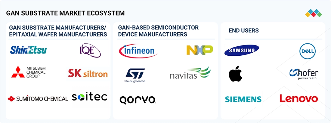
GAN SUBSTRATE MARKET SIZE SHARE ANALYSIS: COMMERCIAL USE CASES ACROSS INDUSTRIES
| COMPANY | USE CASE DESCRIPTION | BENEFITS |
|---|---|---|
 |
Supplies free-standing GaN substrates and GaN epitaxial wafers for RF devices, power semiconductors, laser diodes, and UV optoelectronic applications | Low defect substrates | High thermal conductivity | Improved device efficiency and reliability |
 |
Develops GaN substrates for high-frequency RF amplifiers, power electronics, LEDs, and next-generation semiconductor devices | High breakdown voltage | Superior power density | Reduced switching losses | Longer device lifetime |
 |
Manufactures GaN epitaxial wafers for RF, MicroLED, power electronics, and optical communication applications | High-quality epitaxial layers | Scalable manufacturing | Enhanced device performance |
 |
Offers engineered GaN substrates and epitaxial solutions for RF, power, and photonic semiconductor applications | Improved wafer uniformity | Reduced crystal defects | Enhanced manufacturing compatibility for advanced devices |
 |
Develops engineered GaN-on-insulator (GaNOI) substrates for RF front-end modules, photonics, and power electronics | Improved RF performance | Enhanced thermal management | Improved integration capability | Enhanced system efficiency |
Logos and trademarks shown above are the property of their respective owners. Their use here is for informational and illustrative purposes only.
Related Ecosystem
Communication And Connectivity Technology
- Sensors
- Smart Card & Readers
- Cellular Network
- Femtocell
- Image Sensors
- Cisco Systems, Inc.
- HUAWEI TECHNOLOGIES CO LTD
- Lenovo
- Nokia corporation
- CommScope Holding Company, Inc.
Semiconductor Materials And Components
- Sensors
- Gallium Nitride (GaN)
- Digital Signal Processor (DSP)
- Natural Language Processing (NLP)
- Silicon Carbide
- Texas Instruments Incorporated
- Samsung
- APPLIED MATERIALS, INC.
- Stmicroelectronics
- Lenovo
Key Takeaways
- Rest Of Europe's GaN substrate market is valued at $8.1 million in 2026 and projected to reach $12.6 million by 2031, representing a 7.7% CAGR.
- Rest Of Europe demonstrates steady market growth driven by demand for energy-efficient power electronics and RF applications across the region.
- Rest Of Europe's growth rate of 7.7% reflects regional manufacturing expansion and increasing semiconductor technology adoption.
- Rest Of Europe is positioned as a strategic component of Europe's semiconductor supply chain with emerging production capabilities through 2031.
GaN Substrate Market Report Scope
| Report Metric | Details |
|---|---|
| Base Year | 2026 |
| Fastest Growing Segment | 8-INCH (Wafer Size) |
| Forecast Period | 2026-2031 |
| Growth Rate | CAGR of 12.5% from 2026 to 2031 |
| Largest Segment | DISCRETE (Device Type) |
| Market Size Base Year (Billions) | ~USD 0.62 (2026) |
| Revenue Forecast (Billions) | ~USD 1.11 (2031) |
| Segments Covered | Substrate Type, Wafer Size, Doping Type, Device Type, Type, Application, End Use |
Rest Of Europe GaN Substrate Market Report Segmentation
7 segment dimensions are covered across the global market.
By Substrate Type
- Aigan + Gan
- Free-Standing Gan
- Gan-On-Diamond
- Gan-On-Gan
- Gan-On-Sapphire
- Gan-On-Sic
- Gan-On-Silicon
By Wafer Size
- 2-Inch
- 4-Inch
- 6-Inch
- 8-Inch
By Doping Type
- N-Type Gan
- P-Type Gan
- Semi-Insulating Gan
By Device Type
- Discrete
- Ics
By Type
- Blue Leds
- Green Leds
- Hemt
- Lasers
- Leds
- Other Discrete Devices
- Uv Leds
- Vertical Gan
- White Leds
By Application
- Optoelectronic Devices
- Power Devices
- Rf Devices
By End Use
- Aerospace & Defense
- Automotive
- Consumer Electronics
- Energy & Power
- Healthcare
- Industrial
- Telecommunications
Target Audience
- GaN Substrate Manufacturers : Manufacturers need Rest Of Europe-specific market data to identify regional demand patterns, optimize production capacity, and develop localized supply chain strategies for this growing but moderately-paced market segment.
- Power Electronics OEMs : Original equipment manufacturers in Rest Of Europe require detailed market intelligence to forecast GaN substrate availability, plan component sourcing, and align product roadmaps with regional adoption trends.
- Semiconductor Equipment Suppliers : Equipment and materials suppliers need Rest Of Europe market insights to identify growth opportunities in GaN substrate production infrastructure and plan regional sales and support operations accordingly.
- Investment & Private Equity Firms : Investors evaluating opportunities in European semiconductor and power electronics sectors require Rest Of Europe-specific market data to assess growth potential, competitive dynamics, and valuation benchmarks.
- Technology Strategy Consultants : Consultants advising European industrial and automotive clients need Rest Of Europe GaN market forecasts to develop technology adoption strategies and identify emerging opportunities in power conversion and RF applications.
Reasons to Buy this Report
- Regional Market Sizing : Obtain precise valuation data specific to Rest Of Europe, enabling accurate budget allocation and investment decisions tailored to this distinct regional market segment rather than relying on broader European aggregates.
- Growth Trajectory Insights : Understand the 7.7% CAGR dynamics unique to Rest Of Europe, identifying which countries and applications are driving expansion and where competitive opportunities exist within the region through 2031.
- Application-Specific Demand : Access detailed intelligence on power electronics, RF communications, and emerging semiconductor applications specific to Rest Of Europe, enabling targeted product development and market entry strategies.
- Competitive Positioning : Benchmark your organization against regional competitors and understand Rest Of Europe's market maturity relative to faster-growing regions, informing strategic resource allocation and expansion priorities.
- Investment Decision Support : Make data-driven decisions regarding manufacturing facilities, distribution networks, and R&D investments in Rest Of Europe with confidence in market size projections and growth forecasts through 2031.
Frequently asked questions
What is the market size of GaN substrates in Rest Of Europe in 2026?
Rest Of Europe's GaN substrate market is estimated at $8.1 million in 2026.
What is the projected market size for Rest Of Europe by 2031?
Rest Of Europe's GaN substrate market is forecast to reach $12.6 million by 2031.
What is the CAGR for the GaN substrate market in Rest Of Europe?
Rest Of Europe's GaN substrate market is expected to grow at a compound annual growth rate of 7.7% from 2026 to 2031.
What are the primary drivers of growth in Rest Of Europe's GaN substrate market?
Rest Of Europe's market growth is driven by increasing demand for energy-efficient power conversion, RF applications, and expanding semiconductor manufacturing capabilities across the region.
How does Rest Of Europe's growth compare to the global GaN substrate market?
Rest Of Europe's 7.7% CAGR is more moderate than the global market CAGR of 12.5%, reflecting regional market maturity and manufacturing development patterns.
RESEARCH METHODOLOGY
The study involved major activities in estimating the current market size for the GaN substrate market. Exhaustive secondary research was done to collect information on the market. The next step was to validate these findings and assumptions and validate them with industry experts across the supply chain through primary research. Different approaches, including top-down and bottom-up methods, were employed to estimate the total market size. Following this, the market breakup and data triangulation procedures were employed to determine the market size of the segments and subsegments within the market.
Secondary Research
Secondary research for this study involved gathering information from various credible sources, such as company reports, white papers, journals, and industry publications. This process helps in understanding the supply and value chains, identifying key players, analyzing market segmentation and regional trends, and tracking major market and technology developments. The data collected was used to estimate the overall market size, which was later validated through primary research.
Primary Research
Extensive primary research was conducted after gaining knowledge about the current scenario of the GaN substrate market through secondary research. Several primary interviews were conducted with experts from the demand and supply sides across three major regions—North America, Asia Pacific, Europe, and RoW. This primary data was collected through questionnaires, emails, and telephonic interviews.
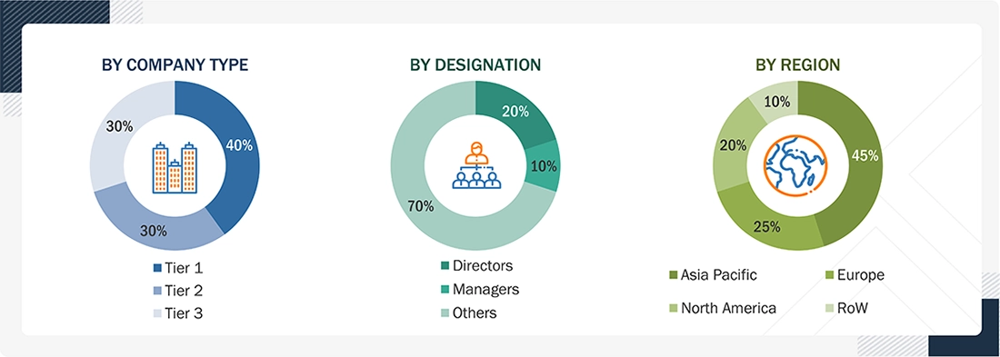
Note: Other designations include product managers, sales managers, and marketing managers.
Tier 1 companies include market players with revenues above USD 500 million; tier 2 companies earn revenues between USD 100 million and USD 500 million; and tier 3 companies earn up to USD 100 million.
To know about the assumptions considered for the study, download the pdf brochure
Market Size Estimation
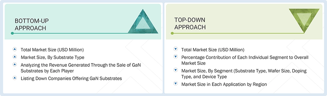
The bottom-up procedure has been employed to arrive at the overall size of the GaN substrate market.
- Identifying GaN substrate types provided or expected to be offered by players in the value chain
- Tracking the major manufacturers and providers of GaN substrate for different regions
- Tracking the ongoing and upcoming product launches and different inorganic strategies, such as acquisitions, partnerships, and collaborations
- Estimating and forecasting the GaN substrate market in each country and, thereby, region based on trade data and GDP analysis
- Conducting multiple discussions with key opinion leaders to understand the types of GaN substrates deployed by market players and analyzing the breakup of the scope of work carried out by each major company
- Verifying and crosschecking the estimates at every level by discussing with key opinion leaders, including CEOs, directors, and operation managers, and then finally with the domain experts at MarketsandMarkets
- Studying various paid and unpaid information sources, such as annual reports, press releases, white papers, and others
The top-down approach has been used to estimate and validate the total size of the GaN substrate market.
- Focusing on top-line investments and expenditures being made in the ecosystems of various end users
- Calculating the market size considering revenues generated by major players through the cost of GaN Substrate
- Segmenting each end user of GaN substrates in each region and deriving the global market size based on region
- Acquiring and analyzing information related to revenues generated by players through their key product offerings
- Conducting multiple on-field discussions with key opinion leaders involved in the development of various GaN substrate wafers and epitaxial wafers
- Estimating the geographic split using secondary sources based on various factors, such as the number of players in a specific country and region and the types of GaN substrates used in RF devices, power devices, and optoelectronics
Data Triangulation
After arriving at the overall market size using the market size estimation processes as explained above, the market has been split into several segments and subsegments. Data triangulation and market breakdown procedures have been employed to complete the entire market engineering process and arrive at the exact statistics of each market segment and subsegment. The data has been triangulated by studying various factors and trends from the demand and supply sides in the GaN substrate market.
Market Definition
The GaN substrate market comprises the global production, supply, and commercialization of gallium nitride (GaN)-based substrates and engineered wafers used as the foundational material for manufacturing high-performance semiconductor devices. The market includes free-standing GaN substrates and GaN epitaxial wafers such as GaN-on-sapphire, GaN-on-silicon, GaN-on-silicon carbide (SiC), GaN-on-GaN, GaN-on-diamond, and AlGaN/GaN structures. These substrates enable the fabrication of power devices, RF devices, and optoelectronic devices by offering superior electrical performance, high breakdown voltage, excellent thermal stability, and high-frequency operation compared to conventional semiconductor materials. GaN caters to end uses including consumer electronics, telecommunications, automotive, aerospace & defense, energy & power, healthcare, and industrial sectors.
Key Stakeholders
- Raw Material Suppliers
- Wafer and Substrate Manufacturers
- Epitaxy Service Providers
- Semiconductor Foundries
- Device Manufacturers
- Research Institutions
- End-use Industries
- Equipment Manufacturers
- Regulatory Bodies
- Distributors and Resellers
Report Objectives
- To describe and forecast the GaN substrate market, by wafer size, substrate type, device type, doping type, application, and end use, in terms of value
- To forecast the market size for various segments with respect to four main regions, namely North America, Europe, Asia Pacific, and RoW, in terms of value
- To describe and forecast wafer sizes for the application segment within the GaN substrate market, in terms of volume
- To provide detailed information regarding the major drivers, restraints, opportunities, and challenges influencing the growth of the GaN substrate market
- To study the complete value chain and related industry segments for the GaN substrate market
- To strategically analyze the micromarkets with respect to individual growth trends, prospects, and contributions to the total market
- To analyze trends and disruptions, pricing trends, investment and funding scenario, patents and innovations, trade data (export and import data), regulatory environment, Porter's five forces analysis, case studies, key stakeholders & buying criteria, technology trends, the market ecosystem, and key conferences and events related to the GaN substrate market
- To strategically analyze micromarkets with regard to individual growth trends, prospects, and contributions to the overall market
- To analyze opportunities in the market for stakeholders by identifying high-growth segments
- To provide details of the competitive landscape for market leaders
- To provide details of the macroeconomic outlook for regions
- To analyze strategies such as product launches, partnerships, collaborations, and acquisitions are adopted by players in the GaN substrate market
- To profile key players in the GaN substrate market and comprehensively analyze their market ranking based on their revenue, market share, and core competencies
Available customizations:
With the given market data, MarketsandMarkets offers customizations according to the company‘s specific needs. The following customization options are available for the report.
Company Information:
- Detailed analysis and profiling of additional market players (up to five)
Get the Full GaN Substrate Market Report
Full forecast, segment splits, and company analysis for all GaN Substrate Market.
- Rest Of Asia Pacific GaN Substrate Market
- Southeast Asia GaN Substrate Market
- Brazil GaN Substrate Market
- Rest Of South America GaN Substrate Market
- GCC GaN Substrate Market
- South Africa GaN Substrate Market
- US GaN Substrate Market
- Canada GaN Substrate Market
- Mexico GaN Substrate Market
- Germany GaN Substrate Market
- UK GaN Substrate Market
- France GaN Substrate Market
- Netherlands GaN Substrate Market
- Italy GaN Substrate Market
- Spain GaN Substrate Market
- China GaN Substrate Market
- Japan GaN Substrate Market
- South Korea GaN Substrate Market
- India GaN Substrate Market
- Taiwan GaN Substrate Market
Need a Tailored Report?
Customize this report to your needs
Get 10% FREE Customization
Customize This Report