
Mexico Semiconductor Ceramic Packaging Materials Market (2025-2030)

The Mexico Semiconductor Ceramic Packaging Materials Market was valued at $13.2 Million in 2025 and projected to reach to $20.8 Million by 2030, representing a compound annual growth rate of 9.4%. Mexico's semiconductor ceramic packaging materials market is poised for accelerated growth through 2030, driven by increasing semiconductor manufacturing activities and Mexico's role as a critical supply chain partner for North American electronics producers.


| Market Size in | USD 26.32 MN |
| Market Forecast in | |
| CAGR | |
| Forecast Period | |
| Units Considered | Value (USD MN) |
Mexico Semiconductor Ceramic Packaging Materials Market Trends and Insights
- Valued at USD 13.2 million in 2025, Mexico's market is expected to expand to USD 20.8 million by 2030, reflecting a compound annual growth rate of 9.4%.
- This growth trajectory outpaces the global average, driven by Mexico's strategic role in semiconductor supply chain localization and increasing foreign direct investment in electronics manufacturing. The expansion of Mexico's semiconductor ceramic packaging materials market is underpinned by rising demand from integrated circuit manufacturers and packaging assembly operations establishing operations in the region.
- Mexico's competitive labor costs, proximity to North American markets, and improving infrastructure have attracted major semiconductor players to establish or expand facilities.
- Between 2025 and 2030, Mexico is expected to capture growing market share as regional semiconductor production scales, particularly in advanced packaging technologies requiring high-performance ceramic substrates and materials..
Key Market Statistics
- CAGR (2025-2030) 9.4% CAGR
- Market Size, 2025 ~USD 13.2 Million
- Forecast, 2030 ~USD 20.8 Million
- Country Mexico
Mexico Semiconductor Ceramic Packaging Materials Market Overview
Market Valuation Growth :
Mexico's semiconductor ceramic packaging materials market is valued at USD 13.2 million in 2025 and is projected to reach USD 20.8 million by 2030, demonstrating robust expansion within the region.
Outpacing Global Growth :
With a CAGR of 9.4%, Mexico's market growth significantly exceeds the global average of 8.5%, positioning the country as a high-growth hub for semiconductor packaging materials in North America.
Strategic Manufacturing Hub :
Mexico's semiconductor ceramic packaging materials sector benefits from its strategic location in North America's advanced manufacturing ecosystem, attracting foreign direct investment and technology transfer.
Supply Chain Integration :
Mexico's proximity to major semiconductor manufacturing facilities and its integration into North American supply chains create sustained demand for high-quality ceramic packaging materials.
Mexico Semiconductor Ceramic Packaging Materials Market Dynamics
- The country's competitive labor costs, established manufacturing infrastructure, and proximity to major markets position it favorably for capturing growing demand from automotive, consumer electronics, and industrial semiconductor applications. Government initiatives supporting advanced manufacturing and foreign investment in semiconductor-related industries are expected to further bolster market expansion.
- As global semiconductor supply chains continue to diversify away from traditional Asian hubs, Mexico is well-positioned to capture incremental demand, with ceramic packaging materials serving as essential components in next-generation semiconductor devices and applications..
Market Ecosystem
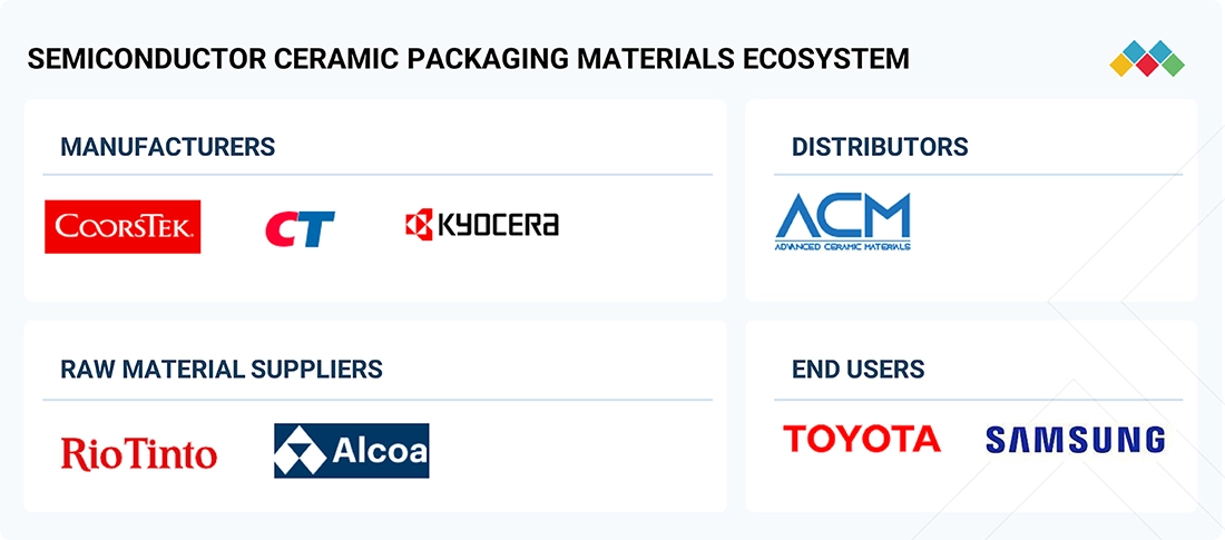
Semiconductor Ceramic Packaging Materials Market: COMMERCIAL USE CASES ACROSS INDUSTRIES
| COMPANY | USE CASE DESCRIPTION | BENEFITS |
|---|---|---|
 |
CoorsTek produces high-performance ceramic materials including alumina, aluminum nitride, silicon nitride, and zirconia for semiconductor packaging, thermal management, and high-power electronics applications. Its materials are supplied as powders, substrates, and custom-engineered components for consumer electronics, automotive, and industrial applications. | CoorsTek provides benefits through its broad material portfolio and high consistency in purity and mechanical properties. Its engineering support enables custom solutions, while its global production footprint ensures a reliable supply for high-volume semiconductor and electronics manufacturers. |
 |
CeramTec manufactures advanced ceramics such as alumina, aluminum nitride, and zirconia for substrates, insulators, and thermal interface components in semiconductor devices and high-power modules. The company also provides precision machining and custom component fabrication. | CeramTec offers high thermal conductivity, mechanical stability, and electrical insulation for critical semiconductor applications. Its ability to provide both standard and custom-engineered ceramic components supports rapid prototyping and scalable production, minimizing material waste and process disruptions. |
 |
Morgan Advanced Materials supplies engineered ceramics including alumina, silicon nitride, aluminum nitride, and boron nitride for electronic substrates, MEMS, and high-frequency semiconductor packages. Its solutions are used in automotive electronics, telecom modules, and industrial power systems. | Morgan’s ceramics provide excellent thermal management and electrical insulation, enhancing device reliability and performance. The company offers technical support for integration into semiconductor assemblies and leverages a global manufacturing network for consistent quality and on-time delivery. |
 |
KYOCERA produces high-performance ceramic materials such as alumina, aluminum nitride, and silicon carbide for substrates, heat sinks, and electronic components in consumer electronics, EV modules, and industrial semiconductor applications. | KYOCERA’s materials are valued for their thermal conductivity, electrical insulation, and precision engineering. The company ensures high-volume production capabilities and provides custom material solutions to optimize performance and device longevity in critical semiconductor applications. |
Logos and trademarks shown above are the property of their respective owners. Their use here is for informational and illustrative purposes only.
Related Ecosystem
Speciality Chemicals
- Corrosion Inhibitors
- Polyetheretherketone (PEEK)
- Acrylonitrile Butadiene Styrene (ABS)
- Epoxy Resin
- Polycarbonate
- Basf se
- DOW CHEMICAL COMPANY
- Evonik industries ag
- Clariant ag.
- Solvay sa
Key Takeaways
- Mexico's semiconductor ceramic packaging materials market is valued at USD 13.2 million in 2025 and is projected to reach USD 20.8 million by 2030, representing a 9.4% CAGR.
- Mexico's market growth rate exceeds the global average of 8.5%, positioning the country as a high-growth region for semiconductor packaging materials in North America.
- Mexico's strategic geographic location, cost competitiveness, and expanding semiconductor manufacturing base are driving increased demand for advanced ceramic packaging materials.
- Supply chain diversification and nearshoring initiatives are accelerating semiconductor packaging operations in Mexico, supporting sustained market expansion through 2030.
Semiconductor Ceramic Packaging Materials Market Report Scope
| Report Metric | Details |
|---|---|
| Base Year | 2025 |
| Fastest Growing Segment | CONSUMER ELECTRONICS (End-Use Industry) |
| Forecast Period | 2025–2030 |
| Growth Rate | CAGR of 8.5% from 2025 to 2030 |
| Largest Segment | SURFACE MOUNT PACKAGES - LEADLESS (Packaging Technology) |
| Market Size Base Year (Billions) | ~USD 1.85 (2025) |
| Revenue Forecast (Billions) | ~USD 2.78 (2030) |
| Segments Covered | Material, Packaging Technology, End-Use Industry |
Mexico Semiconductor Ceramic Packaging Materials Market Report Segmentation
3 segment dimensions are covered across the global market.
By Material
- Alumina
- Aluminum Nitride
- Beryllium Oxide
- Other Materials
- Silicon Carbide
- Silicon Nitride
By Packaging Technology
- Advanced Miniaturized Packages
- Other Packaging Technologies
- Surface Mount Packages - Leaded
- Surface Mount Packages - Leadless
- Through-Hole Packages
By End-Use Industry
- Aerospace & Defense
- Aerospace And Defense
- Automotive
- Consumer Electronics
- Healthcare
- It & Telecommunication
- Other End-Use Industries
MEXICO: SEMICONDUCTOR CERAMIC PACKAGING MATERIALS MARKET, BY END-USE INDUSTRY, 2025–2030
| Segment | 2025 | 2026 | 2027 | 2028 | 2029 | 2030 | CAGR (%) |
|---|---|---|---|---|---|---|---|
| AEROSPACE & DEFENSE | 1.3 | 1.4 | 1.5 | 1.6 | 1.8 | 2 | 8.7 |
| AUTOMOTIVE | 2.9 | 3.2 | 3.5 | 3.8 | 4.2 | 4.6 | 9.6 |
| CONSUMER ELECTRONICS | 4.5 | 4.9 | 5.4 | 5.9 | 6.5 | 7.2 | 10 |
| HEALTHCARE | 1.6 | 1.7 | 1.8 | 2 | 2.2 | 2.4 | 9 |
| IT & TELECOMMUNICATION | 2.4 | 2.6 | 2.8 | 3.1 | 3.3 | 3.7 | 9.1 |
| OTHER END-USE INDUSTRIES | 0.6 | 0.7 | 0.8 | 0.8 | 0.9 | 1 | 8.3 |
| TOTAL | 13.2 | 14.5 | 15.8 | 17.3 | 18.9 | 20.8 | 9.4 |
Target Audience
- Semiconductor Manufacturers : Semiconductor producers operating in or expanding into Mexico require market intelligence to assess ceramic packaging material availability, supplier capabilities, and cost competitiveness for their manufacturing operations.
- Materials & Chemical Suppliers : Ceramic packaging materials suppliers need Mexico-specific market data to evaluate demand potential, identify distribution partnerships, and develop localized product strategies for the region.
- Electronics OEMs : Original equipment manufacturers sourcing semiconductor components from Mexico-based suppliers require insights into local packaging material quality, availability, and supply chain reliability.
- Investment & Private Equity Firms : Investors evaluating opportunities in Mexico's advanced manufacturing and semiconductor sectors need validated market data to assess growth potential and support due diligence for acquisition or expansion targets.
- Government & Trade Organizations : Mexican government agencies and trade bodies require market intelligence to support industrial policy development, foreign investment attraction, and strategic planning for semiconductor ecosystem growth.
Key Companies in the Mexico Semiconductor Ceramic Packaging Materials Market
| Company | HQ | Ownership | Strongest segments |
|---|---|---|---|
| KYOCERA CORPORATION | Japan | Public Company | Core Components Business (fine ceramics, packages, optical and medical components),Electronic Components Business (sensors, capacitors, crystal devices, connectors, power semiconductors),Solutions Business – printers, MFPs, commercial inkjet, document solutions, |
| COORSTEK | United States | Private Company | Semiconductor and electronic components,Medical and life sciences components,Aerospace and defense components, |
| MORGAN ADVANCED MATERIALS | United Kingdom | Public Company | Thermal Products,Performance Carbon,Technical Ceramics, |
| NGK INSULATORS, LTD. | Japan | Public Company | Power insulators and grid equipment,Automotive emissions ceramics and sensors,Digital society ceramics and substrates, |
| MARUWA CO., LTD. | Japan | Public Company | Ceramic substrates and components (including SiC, AlN, hermetic seals),Electronic components and devices (antennas, EMC/RF components, capacitors),Semiconductor quartz glass products (tubes, boats, related), |
| AGC INC. | United States | Public Company | High-horsepower and utility tractors,Compact tractors and specialty equipment,Combines and harvesting equipment, |
| MATERION CORPORATION | United States | Public Company | Performance Materials (beryllium and copper-based alloys, ToughMet, SupremEX, precision strip),Electronic Materials (advanced chemicals, vapor deposition targets, microelectronics packaging),Precision Optics (thin film coatings, optical filters, assemblies), |
| TOKUYAMA CORPORATION | Japan | Public Company | Chemicals Products (caustic soda, chlor-alkali, PVC chain, solvents),Cement and Building Materials,Electronics Advanced Materials (poly-Si, silica, AIN, BN, high-purity chemicals), |
| FERROTEC CORPORATION | Japan | Public Company | Semiconductor equipment-related products and vacuum components,Power electronic substrates and related technologies,Thermoelectric modules and micro thermoelectric modules, |
KYOCERA CORPORATION
Kyocera Corporation is a Japanese public company founded in 1946 with 73,856 employees. The company operates as a diversified manufacturer with significant global operations.
COORSTEK
CoorsTek is a United States-based private company founded in 1910 with 2,361 employees. The company is a manufacturer of engineered ceramics and materials.
MORGAN ADVANCED MATERIALS
Morgan Advanced Materials is a United Kingdom-based public company founded in 1856 with 8,088 employees. The company specializes in advanced materials and thermal management solutions.
NGK INSULATORS, LTD.
NGK Insulators, Ltd. is a Japanese public company founded in 1919 with 19,869 employees. The company manufactures insulators and advanced ceramic products.
MARUWA CO., LTD.
Maruwa Co., Ltd. is a Japanese public company founded in 1973 with 2,328 employees. The company produces ceramic and electronic components.
AGC INC.
AGC Inc. is a United States-based public company founded in 1990 with 22,000 employees. The company operates in the advanced materials and specialty chemicals sectors.
MATERION CORPORATION
Materion Corporation is a United States-based public company founded in 1921 with 2,880 employees. The company manufactures advanced materials and engineered products.
TOKUYAMA CORPORATION
Tokuyama Corporation is a Japanese public company founded in 1918 with 6,390 employees. The company produces chemicals, materials, and specialty products.
FERROTEC CORPORATION
Ferrotec Corporation is a Japanese public company founded in 1980 with 16,858 employees. The company manufactures advanced materials and thermal management solutions.
Reasons to Buy this Report
- Market Entry Strategy : Gain comprehensive insights into Mexico's semiconductor ceramic packaging materials market dynamics to develop targeted market entry strategies and identify optimal positioning opportunities within this high-growth segment.
- Competitive Intelligence : Access detailed analysis of Mexico's market landscape, including key players, competitive positioning, and market share distribution to inform strategic business decisions and competitive benchmarking.
- Investment Decision Support : Leverage validated market sizing, growth projections, and CAGR data specific to Mexico to support investment decisions, capital allocation, and business case development for semiconductor packaging initiatives.
- Supply Chain Optimization : Understand Mexico's role within North American semiconductor supply chains and identify opportunities to optimize sourcing, manufacturing, and distribution strategies for ceramic packaging materials.
- Growth Opportunity Identification : Identify emerging applications, end-user segments, and geographic sub-markets within Mexico that present the highest growth potential and return on investment through 2030.
Frequently asked questions
What is the current market size of semiconductor ceramic packaging materials in Mexico?
Mexico's semiconductor ceramic packaging materials market is valued at USD 13.2 million in 2025 and is expected to grow to USD 20.8 million by 2030.
What is the projected growth rate for Mexico's semiconductor ceramic packaging materials market?
Mexico's market is projected to grow at a compound annual growth rate (CAGR) of 9.4% from 2025 to 2030, outpacing the global average of 8.5%.
Why is Mexico's semiconductor ceramic packaging materials market growing faster than the global average?
Mexico's accelerated growth is driven by nearshoring trends, foreign direct investment in semiconductor manufacturing, competitive labor costs, and strategic proximity to North American markets.
What are the primary applications of ceramic packaging materials in Mexico's semiconductor industry?
Ceramic packaging materials in Mexico are primarily used for integrated circuit substrates, thermal management solutions, and advanced packaging technologies in semiconductor assembly operations.
Which industries are driving demand for semiconductor ceramic packaging materials in Mexico?
Demand is driven by semiconductor manufacturing, integrated circuit packaging, automotive electronics, consumer electronics, and telecommunications equipment production in Mexico.
RESEARCH METHODOLOGY
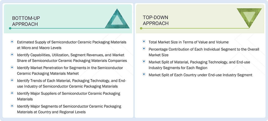
The study involved four major activities in estimating the market size of the semiconductor ceramic packaging materials market. Exhaustive secondary research was done to collect information on the market, the peer market, and the parent market. The next step was to validate these findings, assumptions, and sizing with industry experts across the value chain through primary research. Both top-down and bottom-up approaches were employed to estimate the complete market size. Thereafter, the market breakdown and data triangulation procedures were used to estimate the market size of the segments and subsegments.
Secondary Research
In the secondary research process, various secondary sources have been referred to for identifying and collecting information for this study. These secondary sources include annual reports, press releases, investor presentations of companies, white papers, certified publications, trade directories, certified publications, articles from recognized authors, gold standard and silver standard websites, and databases.
Secondary research has been used to obtain key information about the value chain of the industry, monetary chain of the market, the total pool of key players in the semiconductor ceramic packaging materials, market classification and segmentation according to industry trends to the bottom-most level, and regional markets. It was also used to obtain information about the key developments from a market-oriented perspective.
Primary Research
The semiconductor ceramic packaging materials market comprises several stakeholders in the value chain, which include raw material suppliers, manufacturers, and end users. Various primary sources from the supply and demand sides of the semiconductor ceramic packaging materials market have been interviewed to obtain qualitative and quantitative information. The primary interviewees from the demand side include key opinion leaders in end-use sectors. The primary sources from the supply side include manufacturers, associations, and institutions involved in the semiconductor ceramic packaging materials industry.
Primary interviews were conducted to gather insights such as market statistics, data of revenue collected from the products and services, market breakdowns, market size estimations, market forecasting, and data triangulation. Primary research also helped in understanding the various trends related to material, packaging technology, end-use industry, and region. Stakeholders from the demand side, such as CIOs, CTOs, and CSOs were interviewed to understand the buyer’s perspective on the suppliers, products, component providers, and their current usage of semiconductor ceramic packaging materials and future outlook of their business which will affect the overall market.
The breakdown of profiles of the primary interviewees is illustrated in the figure below:
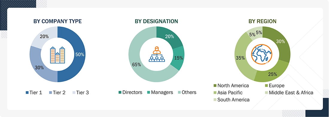
Note: Tier 1, Tier 2, and Tier 3 companies are classified based on their market revenue in 2024, which is available in the public domain, their product portfolios, and their geographical presence.
Other designations include sales representatives, production heads, and technicians.
To know about the assumptions considered for the study, download the pdf brochure
Market Size Estimation
The top-down approach was used to estimate and validate the size of various submarkets for semiconductor ceramic packaging materials for each region. The research methodology used to estimate the market size included the following steps:
- The key players in the industry have been identified through extensive secondary research.
- The supply chain of the industry has been determined through primary and secondary research.
- The global market was then segmented into five major regions and validated by industry experts.
- All percentage shares, splits, and breakdowns based on material, packaging technology, end-use industry, and regions were determined using secondary sources and verified through primary sources.
- All possible parameters that affect the markets covered in this research study were accounted for, viewed in extensive detail, verified through primary research, and analyzed to get the final quantitative and qualitative data. This data was consolidated and added with detailed inputs and analysis, and presented in this report.
Data Triangulation
After arriving at the total market size from the estimation process in the semiconductor ceramic packaging materials above, the overall market has been split into several segments and subsegments. To complete the overall market engineering process and arrive at the exact statistics for all the segments and subsegments, the data triangulation and market breakdown procedures have been employed, wherever applicable. The data has been triangulated by studying various factors and trends from both the demand and supply sides. Along with this, the market size has been validated by using both the top-down and bottom-up approaches and primary interviews. Hence, for every data segment, there have been three sources: the top-down approach, the bottom-up approach, and expert interviews. The data was assumed correct when the values arrived from the three sources matched.
Market Definition
The semiconductor ceramic packaging materials market refers to the industry segment focused on the production and supply of ceramic materials used to package semiconductor devices, such as integrated circuits (ICs), power modules, sensors, and micro-electromechanical systems (MEMS). Ceramic packaging provides critical advantages over traditional plastic or metal alternatives, including high thermal conductivity, excellent electrical insulation, mechanical strength, and resistance to moisture, corrosion, and extreme environmental conditions. These properties make ceramic materials indispensable for applications where reliability, durability, and performance are crucial, such as in automotive electronics, aerospace systems, defense equipment, and high-performance computing. The market encompasses various types of ceramics, including alumina, aluminum nitride, and beryllium oxide, each offering specific benefits such as superior heat dissipation, insulation, or mechanical robustness. Increasing miniaturization and power density of semiconductor devices are driving higher demand for ceramic packaging solutions that can manage heat efficiently while maintaining device integrity.
Stakeholders
- Semiconductor Ceramic Packaging Material Manufacturers
- Semiconductor Ceramic Packaging Material Traders, Distributors, and Suppliers
- Raw Material Suppliers
- Government and Private Research Organizations
- Associations and Industrial Bodies
- R&D Institutions
- Environmental Support Agencies
Report Objectives
- To define, describe, and forecast the size of the semiconductor ceramic packaging materials market, in terms of value and volume
- To provide detailed information regarding the major factors (drivers, opportunities, restraints, and challenges) influencing the growth of the market
- To estimate and forecast the market size based on material, packaging technology, end-use industry, and region
- To forecast the size of the market with respect to major regions, namely, Europe, North America, Asia Pacific, Middle East & Africa, and South America, along with their key countries
- To strategically analyze micromarkets with respect to individual growth trends, prospects, and their contribution to the overall market.
- To analyze opportunities in the market for stakeholders and provide a competitive landscape of market leaders
- To track and analyze recent developments such as product launches, partnerships, and expansions in the market
- To strategically profile the key market players and comprehensively analyze their core competencies
Get the Full Semiconductor Ceramic Packaging Materials Market Report
Full forecast, segment splits, and company analysis for all Semiconductor Ceramic Packaging Materials Market.
- China Semiconductor Ceramic Packaging Materials Market
- Japan Semiconductor Ceramic Packaging Materials Market
- India Semiconductor Ceramic Packaging Materials Market
- South Korea Semiconductor Ceramic Packaging Materials Market
- Taiwan Semiconductor Ceramic Packaging Materials Market
- US Semiconductor Ceramic Packaging Materials Market
- Canada Semiconductor Ceramic Packaging Materials Market
- Germany Semiconductor Ceramic Packaging Materials Market
- UK Semiconductor Ceramic Packaging Materials Market
- France Semiconductor Ceramic Packaging Materials Market
- Italy Semiconductor Ceramic Packaging Materials Market
- Spain Semiconductor Ceramic Packaging Materials Market
- South Africa Semiconductor Ceramic Packaging Materials Market
- Argentina Semiconductor Ceramic Packaging Materials Market
- Brazil Semiconductor Ceramic Packaging Materials Market
- Rest Of Asia Pacific Semiconductor Ceramic Packaging Materials Market
Need a Tailored Report?
Customize this report to your needs
Get 10% FREE Customization
Customize This Report