
Semiconductor Ceramic Packaging Materials Market

Semiconductor Ceramic Packaging Materials Market by Material (Alumina, Aluminum Nitride, Silicon Nitride, Silicon Carbide, Beryllium Oxide), Packaging Technology (Through-Hole Packages, Surface Mount Packages � Leaded, Surface Mount Packages � Leadless, Advanced Miniaturized Packages), End-use Industry (Consumer Electronics, Automotive, Healthcare, IT & Telecommunication, Aerospace and Defense), & Region - Global Forecast to 2030


OVERVIEW
Source: Secondary Research, Interviews with Experts, MarketsandMarkets Analysis
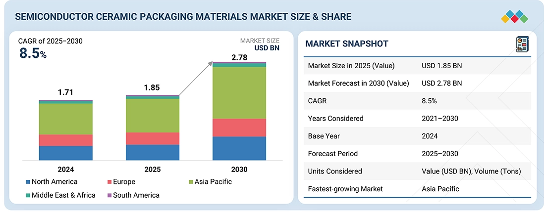
The semiconductor ceramic packaging materials market size is projected to grow from USD 1.85 billion in 2025 to USD 2.78 billion by 2030, registering a CAGR of 8.5% during the forecast period. Semiconductor ceramic packaging materials include high-performance ceramics such as alumina, aluminum nitride, and silicon nitride, which are widely recognized for their excellent thermal conductivity, electrical insulation, and mechanical stability. These materials serve as critical enablers in protecting semiconductor devices, ensuring reliable heat dissipation, and maintaining signal integrity in advanced electronic applications. The market growth for semiconductor ceramic packaging materials is being fueled by increasing demand in sectors such as automotive electronics, consumer electronics, telecommunications, and industrial electronics, where high-reliability and miniaturized semiconductor packages are essential.
KEY TAKEAWAYS
-
BY MATERIALThe semiconductor ceramic packaging materials market is segmented into alumina, aluminum nitride, silicon nitride, silicon carbide, beryllium oxide, and other materials. Alumina holds the largest share due to its cost-effectiveness, excellent thermal stability, and widespread use in standard semiconductor packages. Aluminum nitride and silicon nitride are preferred in high-performance applications requiring superior thermal conductivity and mechanical strength, while silicon carbide and beryllium oxide are employed in specialized, high-reliability applications.
-
BY PACKAGING TECHNOLOGYThe market is classified by packaging technology into through-hole packages, surface mount packages – leaded, surface mount packages – leadless, advanced miniaturized packages, and other packaging technologies. Surface mount packages – leadless dominate the market due to their compact design, ease of automated assembly, and suitability for high-density electronic devices. Advanced miniaturized packages are witnessing rapid growth as device miniaturization and high-performance requirements continue to rise.
-
BY END-USE INDUSTRYConsumer electronics drive the demand for semiconductor ceramic packaging materials, owing to the proliferation of smartphones, tablets, and wearable devices. It is followed by automotive, IT & telecommunication, healthcare, aerospace and defense, and other end-use industries. Growth in these sectors, coupled with increasing adoption of high-reliability, thermally efficient semiconductor packages, fuels steady demand for ceramic packaging materials across industries.
-
COMPETITIVE LANDSCAPEThe semiconductor ceramic packaging materials market is shaped by product launches, partnerships, and expansions among global leaders. Key players include KYOCERA Corporation (Japan), CeramTec GmbH (Germany), CoorsTek (US), Materion Corporation (US), Resonac Holdings Corporation (Japan), NGK INSULATORS, LTD. (Japan), AGC Inc. (Japan), Morgan Advanced Materials (UK), MARUWA Co., Ltd. (Japan), and Tokuyama Corporation (Japan).
The semiconductor ceramic packaging materials market is expected to witness steady growth over the coming years, driven by increasing demand across key end-use industries such as automotive electronics, consumer electronics, telecommunications, and healthcare. Semiconductor ceramic packaging materials are valued for their excellent thermal conductivity, electrical insulation, and mechanical stability, making them essential in protecting semiconductor devices, enabling efficient heat dissipation, and ensuring signal integrity in advanced electronic applications. Expansion of the electronics and automotive sectors globally, coupled with rising adoption of miniaturized and high-reliability semiconductor packages, further supports market growth.
TRENDS & DISRUPTIONS IMPACTING CUSTOMERS' CUSTOMERS
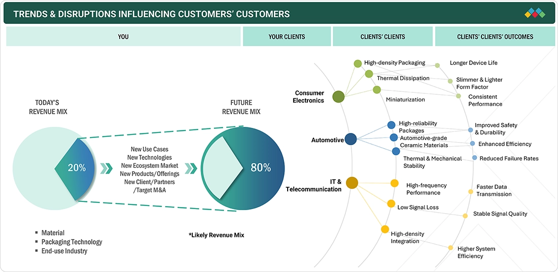
The semiconductor ceramic packaging materials market is witnessing key disruptions driven by technological advancements, regulatory requirements, and evolving demand patterns. In the automotive and consumer electronics sectors, the push for miniaturized, high-reliability, and thermally efficient packages is accelerating the adoption of advanced ceramic materials such as aluminum nitride and silicon nitride. In the IT & telecommunication industry, increasing data transfer speeds and high-power device applications are driving innovations in package design and material performance. Additionally, stringent environmental regulations are prompting manufacturers to optimize material compositions and reduce hazardous elements. These trends highlight how semiconductor ceramic packaging materials are becoming critical enablers of device performance, durability, and regulatory compliance across multiple high-tech industries.
Source: Secondary Research, Interviews with Experts, MarketsandMarkets Analysis
MARKET DYNAMICS
Level
-
Growth in 5G infrastructure and RF devices to increase demand for low-loss ceramic materials

-
Expansion of automotive electronics and EV power modules to boost ceramic packaging adoption

Level
-
High cost of ceramic packaging materials compared to polymer or metal-based packaging

Level
-
Regional localization of semiconductor manufacturing encouraging investment

-
Advanced multilayer ceramic materials for emerging 2.5D/3D semiconductor packaging

Level
-
Difficulty in bonding to dissimilar materials

-
Limited design flexibility of ceramic materials makes fabricating complex geometries challenging

Source: Secondary Research, Interviews with Experts, MarketsandMarkets Analysis
Driver: Expansion of automotive electronics and EV power modules boosting ceramic packaging adoption
The expansion of automotive electronics and the rapid adoption of electric vehicles (EVs) are significantly increasing the demand for semiconductor ceramic packaging materials. Modern vehicles, particularly EVs, rely heavily on high-performance electronic systems for power management, battery control, infotainment, advanced driver-assistance systems (ADAS), and safety functions. These applications generate substantial heat and operate under high electrical loads, requiring packaging materials that provide excellent thermal conductivity, electrical insulation, and mechanical stability. Ceramic materials such as aluminum nitride, silicon nitride, and alumina are particularly suited for these demanding conditions, enabling efficient heat dissipation and protecting sensitive semiconductor components from thermal and mechanical stress. As the automotive industry continues to integrate more electronics and shift toward electrification, the need for reliable, miniaturized, and high-performance packages is growing rapidly. Furthermore, the trend toward higher voltage EV power modules necessitates packaging materials that can withstand extreme operating conditions while maintaining long-term reliability. This drives automotive manufacturers and semiconductor suppliers to increasingly adopt ceramic packaging solutions, directly contributing to market growth.
Restraint: High cost of ceramic packaging materials compared to polymer or metal-based packaging
The high cost of ceramic packaging materials compared to polymer or metal-based alternatives is a significant factor restraining demand in the semiconductor ceramic packaging materials market. Ceramic materials such as alumina, aluminum nitride, and silicon nitride require complex manufacturing processes, including precision sintering, machining, and surface finishing, which increase production costs. Additionally, the specialized equipment and stringent quality control measures needed to produce high-performance ceramic substrates and packages add to the overall expense. In contrast, polymer- and metal-based packaging options are relatively cheaper to manufacture, offer greater flexibility in design, and can be produced in high volumes with lower capital investment, making them attractive for cost-sensitive applications. For many consumer electronics and industrial applications, where performance requirements are moderate, these lower-cost alternatives can meet functional needs while keeping overall product costs down. As a result, manufacturers may hesitate to adopt ceramic packaging unless the application demands its superior thermal, electrical, or mechanical properties. This cost sensitivity is particularly pronounced in emerging markets and price-competitive segments, where the high upfront and production costs of ceramic packaging limit widespread adoption. Consequently, the premium pricing of ceramic materials continues to act as a key restraint on market growth despite their technical advantages.
Opportunity: Regional localization of semiconductor manufacturing encouraging investment
The regional localization of semiconductor manufacturing presents a significant growth opportunity for the semiconductor ceramic packaging materials market. Governments and companies across North America, Europe, and Asia are investing heavily in domestic semiconductor fabrication facilities to reduce reliance on global supply chains, enhance technological sovereignty, and mitigate risks from geopolitical tensions and disruptions. This localization trend drives demand for high-quality packaging materials close to the point of semiconductor production. Ceramic packaging materials, known for their superior thermal conductivity, electrical insulation, and mechanical stability, are essential for high-performance semiconductor devices used in automotive electronics, industrial applications, telecommunications, and consumer electronics. As new fabs and assembly facilities are established, there is an increased need for locally sourced, reliable, and high-performance packaging materials, creating opportunities for ceramic packaging manufacturers to expand production capacities, set up regional supply chains, and partner with semiconductor manufacturers. Furthermore, localized manufacturing enables faster response to market demand, reduces logistics costs, and facilitates customized solutions for specific applications, enhancing the adoption of ceramic packages. Overall, the strategic shift toward regional semiconductor production not only increases immediate demand for ceramic packaging materials but also fosters long-term partnerships and innovation, positioning manufacturers to capture a larger share of a growing, decentralized market.
Challenge: Difficulty in bonding to dissimilar materials
The difficulty in bonding ceramic packaging materials to dissimilar materials represents a significant challenge for the semiconductor ceramic packaging materials market. Ceramics such as alumina, aluminum nitride, and silicon nitride possess high hardness, low thermal expansion coefficients, and chemical inertness, making them excellent for thermal management and electrical insulation. However, these same properties create compatibility issues when joining ceramics with metals, polymers, or other semiconductor materials during device assembly. Differences in thermal expansion between ceramics and metals, for example, can induce stress at the interface during heating or cooling cycles, leading to microcracks, delamination, or component failure. Similarly, achieving reliable adhesion with polymers or composite materials often requires complex surface treatments, specialized adhesives, or intermediate layers, which increase production time and cost. These bonding challenges can limit design flexibility, reduce manufacturing yields, and constrain the adoption of ceramic packages in applications requiring heterogeneous material integration, such as advanced power modules, high-density electronic devices, or multi-material assemblies.
Semiconductor Ceramic Packaging Materials Market: COMMERCIAL USE CASES ACROSS INDUSTRIES
| COMPANY | USE CASE DESCRIPTION | BENEFITS |
|---|---|---|
 |
CoorsTek produces high-performance ceramic materials including alumina, aluminum nitride, silicon nitride, and zirconia for semiconductor packaging, thermal management, and high-power electronics applications. Its materials are supplied as powders, substrates, and custom-engineered components for consumer electronics, automotive, and industrial applications. | CoorsTek provides benefits through its broad material portfolio and high consistency in purity and mechanical properties. Its engineering support enables custom solutions, while its global production footprint ensures a reliable supply for high-volume semiconductor and electronics manufacturers. |
 |
CeramTec manufactures advanced ceramics such as alumina, aluminum nitride, and zirconia for substrates, insulators, and thermal interface components in semiconductor devices and high-power modules. The company also provides precision machining and custom component fabrication. | CeramTec offers high thermal conductivity, mechanical stability, and electrical insulation for critical semiconductor applications. Its ability to provide both standard and custom-engineered ceramic components supports rapid prototyping and scalable production, minimizing material waste and process disruptions. |
 |
Morgan Advanced Materials supplies engineered ceramics including alumina, silicon nitride, aluminum nitride, and boron nitride for electronic substrates, MEMS, and high-frequency semiconductor packages. Its solutions are used in automotive electronics, telecom modules, and industrial power systems. | Morgan’s ceramics provide excellent thermal management and electrical insulation, enhancing device reliability and performance. The company offers technical support for integration into semiconductor assemblies and leverages a global manufacturing network for consistent quality and on-time delivery. |
 |
KYOCERA produces high-performance ceramic materials such as alumina, aluminum nitride, and silicon carbide for substrates, heat sinks, and electronic components in consumer electronics, EV modules, and industrial semiconductor applications. | KYOCERA’s materials are valued for their thermal conductivity, electrical insulation, and precision engineering. The company ensures high-volume production capabilities and provides custom material solutions to optimize performance and device longevity in critical semiconductor applications. |
Logos and trademarks shown above are the property of their respective owners. Their use here is for informational and illustrative purposes only.
MARKET ECOSYSTEM
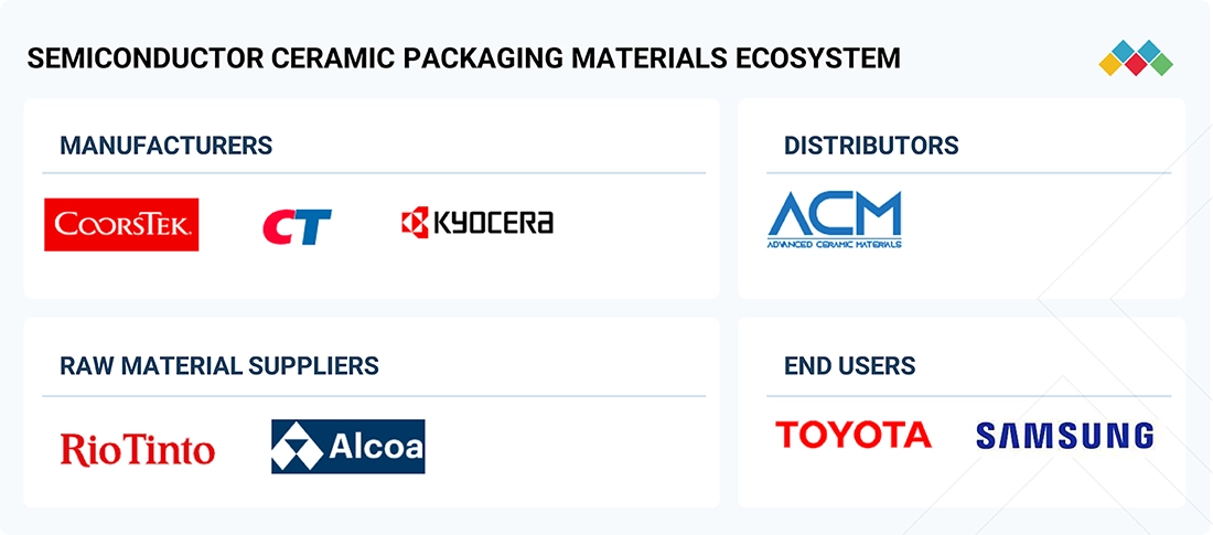
The semiconductor ceramic packaging materials ecosystem involves identifying and analyzing the interconnected relationships among various stakeholders, including raw material suppliers, ceramic material manufacturers, distributors, and end users. Raw material suppliers provide high-purity powders and precursor chemicals necessary for producing ceramic materials such as alumina, aluminum nitride, silicon nitride, and silicon carbide. Manufacturers process these raw materials using techniques such as sintering, pressing, and surface finishing to produce high-performance ceramic substrates and components that meet thermal, electrical, and mechanical specifications. Distributors and suppliers act as intermediaries, ensuring a steady supply of these materials to end users while optimizing inventory and lead times. End users, including semiconductor manufacturers in automotive electronics, consumer electronics, telecommunications, and aerospace, rely on these materials for reliable performance in advanced semiconductor devices.
Logos and trademarks shown above are the property of their respective owners. Their use here is for informational and illustrative purposes only.
MARKET SEGMENTS
Source: Secondary Research, Interviews with Experts, MarketsandMarkets Analysis
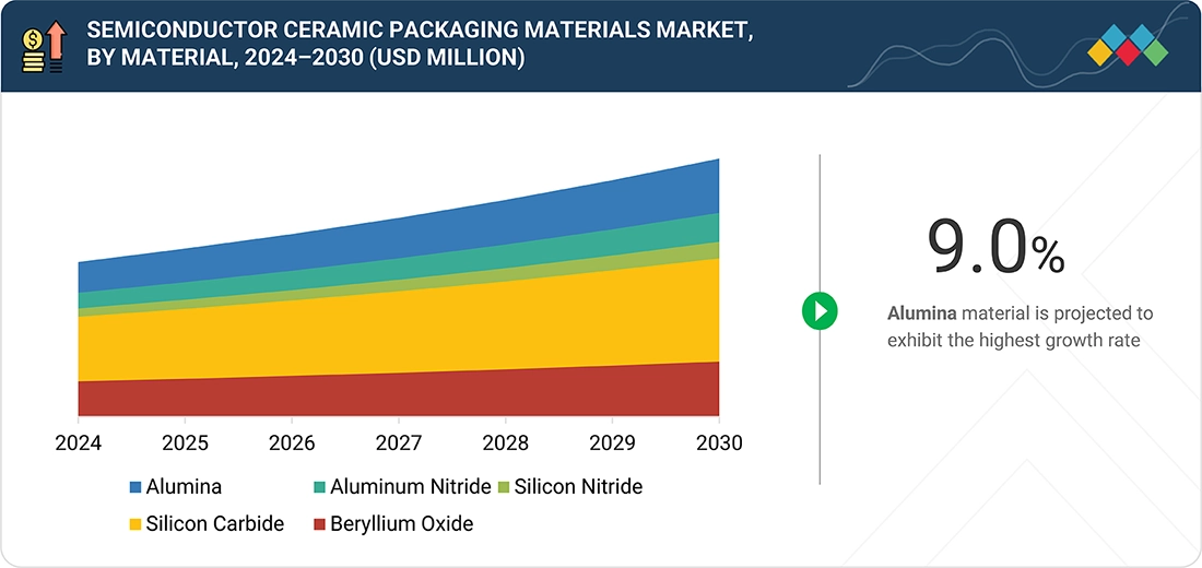
Semiconductor Ceramic Packaging Materials Market, by Material
Alumina accounts for the largest share in the semiconductor ceramic packaging materials market due to its combination of cost-effectiveness, excellent thermal and electrical properties, and widespread applicability across various semiconductor devices. It offers high electrical insulation, good thermal conductivity, and strong mechanical stability, making it suitable for standard substrates, multilayer ceramic packages, and electronic components in consumer electronics, automotive, IT & telecommunications, and industrial applications. Compared to other ceramic materials such as aluminum nitride or silicon nitride, alumina is relatively less expensive to produce and easier to process using established manufacturing techniques such as pressing and sintering, which enables high-volume production and cost efficiency. Its versatility allows it to meet the performance requirements of a broad range of devices without the need for specialized or high-cost handling, making it a preferred choice for manufacturers seeking reliable performance at moderate costs. Additionally, alumina’s long-standing use in the electronics industry has established robust supply chains, technical expertise, and quality standards, further reinforcing its dominance. The combination of affordability, reliable thermal and electrical performance, and broad applicability ensures that alumina continues to hold the largest market share in the semiconductor ceramic packaging materials sector.
Semiconductor Ceramic Packaging Materials Market, by Packaging Technology
Surface mount package – leadless technology accounts for the largest share in the semiconductor ceramic packaging materials market because it requires high-performance ceramic substrates that can support miniaturized, high-density, and high-reliability electronic assemblies. Leadless designs demand precise thermal management, electrical insulation, and mechanical stability to ensure device performance, as there are no leads to dissipate heat or absorb mechanical stress. Ceramic materials such as alumina, aluminum nitride, and silicon nitride are ideal for this technology because they provide excellent thermal conductivity, withstand high power densities, and maintain structural integrity in compact layouts. The increasing adoption of leadless surface-mount packaging technology in automotive electronics, consumer devices, telecommunications, and industrial applications further drives the demand for these ceramic materials. Additionally, this technology supports automated assembly processes, high-frequency operation, and dense multi-layer configurations, which rely heavily on ceramics to maintain signal integrity and device reliability. The combination of material performance requirements, device miniaturization trends, and growing adoption of leadless designs positions this technology as the primary driver of ceramic material consumption in the semiconductor packaging market.
Semiconductor Ceramic Packaging Materials Market, by End-use Industry
Consumer electronics account for the largest share in the semiconductor ceramic packaging materials market due to the rapid growth and continuous innovation in devices such as smartphones, laptops, tablets, wearables, and smart home products. These devices demand high-performance semiconductor components that can handle increasing processing power, higher operating frequencies, and intense heat dissipation within compact form factors. The push for miniaturization and high-density circuit integration requires packaging solutions that maintain reliability under thermal and mechanical stress. Additionally, the surge in connected devices, 5G-enabled technologies, and portable electronics has significantly increased the production volume of semiconductors, thereby boosting the consumption of supporting packaging materials. Asia Pacific, in particular, dominates the production of consumer electronics, creating strong regional demand for high-performance materials to meet quality, durability, and efficiency standards. The combination of technological advancements, growing device penetration, and the need for reliable, high-performance packaging solutions drives sustained demand, positioning consumer electronics as the leading end-use segment and the largest contributor to the growth of the semiconductor ceramic packaging materials market.
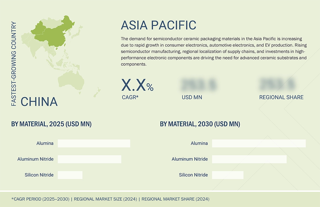
REGION
Asia Pacific to be largest region in global semiconductor ceramic packaging materials market during forecast period
Asia Pacific accounts for the largest share in the semiconductor ceramic packaging materials market due to the region’s strong concentration of semiconductor manufacturing, advanced electronics production, and rapid industrial growth. China leads as a global hub for consumer electronics, automotive electronics, and industrial electronics, creating high demand for ceramic materials for substrates and components. Taiwan and South Korea are home to some of the world’s largest semiconductor fabrication and assembly companies, which rely heavily on high-performance ceramic materials for thermal management, electrical insulation, and mechanical reliability. Japan contributes through its advanced materials industry and precision manufacturing capabilities, supplying high-purity ceramics and specialized powders for demanding applications. The region also benefits from integrated supply chains, abundant raw material availability, and cost-efficient manufacturing infrastructure, which reduces lead times and production costs. Moreover, government initiatives such as China’s “Made in China 2025” and South Korea’s semiconductor investment incentives promote local production and technology development. The combination of high semiconductor production, growing electronics and automotive sectors, and supportive industrial policies positions Asia Pacific as the dominant regional market for semiconductor ceramic packaging materials.
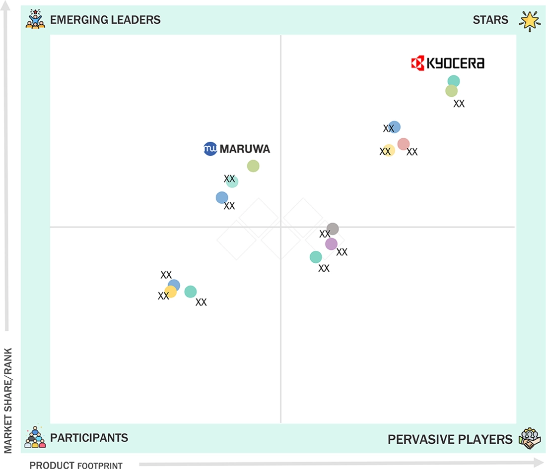
Semiconductor Ceramic Packaging Materials Market: COMPANY EVALUATION MATRIX
The semiconductor ceramics packaging material market is characterized by a mix of emerging leaders, participants, pervasive players, and stars. The chart highlights KYOCERA Corporation as a strong market leader in terms of both market share and product footprint, positioning it in the "Stars" quadrant. MARUWA Co., Ltd. falls within the Emerging Leaders quadrant. Several smaller players cluster in the "Participants" and "Pervasive Players" zones, reflecting niche positioning or early-stage growth potential. Overall, market dynamics suggest strong competition, with global giants driving innovation while smaller companies strive for differentiation and market penetration.
Source: Secondary Research, Interviews with Experts, MarketsandMarkets Analysis
KEY MARKET PLAYERS
MARKET SCOPE
| REPORT METRIC | DETAILS |
|---|---|
| Market Size in 2024 (Value) | USD 1.71 Billion |
| Market Forecast in 2030 (Value) | USD 2.78 Billion |
| Growth Rate | CAGR of 8.5% from 2025–2030 |
| Years Considered | 2021–2030 |
| Base Year | 2024 |
| Forecast Period | 2025–2030 |
| Units Considered | Value (USD Million), Volume (Tons) |
| Report Coverage | Revenue Forecast, Company Ranking, Competitive Landscape, Growth Factors, and Trends |
| Segments Covered |
|
| Regions Covered | Asia Pacific, North America, Europe, Middle East & Africa, and South America |
WHAT IS IN IT FOR YOU: Semiconductor Ceramic Packaging Materials Market REPORT CONTENT GUIDE
DELIVERED CUSTOMIZATIONS
We have successfully delivered the following deep-dive customizations:
| CLIENT REQUEST | CUSTOMIZATION DELIVERED | VALUE ADDS |
|---|---|---|
| Country-level Breakdown | Instead of just regional coverage, the report can provide country-specific market data (e.g., India, Brazil, Saudi Arabia, South Africa, and Mexico). This includes demand drivers, production capacities, import/export trends, and regulatory outlooks. | Helps companies identify high-growth national markets and plan market entry strategies with greater accuracy. |
| Application-specific Deep Dive | Detailed segmentation and insights on key end-use industries such as consumer electronics, automotive, IT & telecom, aerospace & defense, and healthcare. Covers adoption trends, growth forecasts, and industry-specific requirements for ceramic materials. | Supports companies in targeting the most relevant industries, optimizing sales strategies, and aligning material supply with specific industry demands. |
| Purity Customization | Comparative analysis of key materials, including alumina, aluminum nitride, silicon nitride, silicon carbide, and other materials. Covers performance benchmarks, technical advantages, pricing, and suitability for different end-use applications. | Enables manufacturers and buyers to select the optimal material for performance, cost, and reliability, improving product design and supply chain decisions. |
| Competitive Benchmarking | Extended profiling of regional, niche, and global material suppliers (Kyocera, CoorsTek, CeramTec, and Morgan Advanced Materials). Includes SWOT analysis, product differentiation, technology focus, and market positioning. | Provides a clear competitive landscape, helping clients identify potential partners, acquisition targets, or competitive threats based on material type and end-use focus. |
RECENT DEVELOPMENTS
- September 2024 : KYOCERA Corporation inaugurated a new production facility at the Minami Isahaya Industrial Park in Isahaya City, Nagasaki Prefecture. The facility focuses on manufacturing fine ceramic components for semiconductor-related applications and packaging. This expansion enhances the company’s production capacity, enabling it to better meet the growing market demand for its high-performance ceramic products.
- June 2024 : CeramTec GmbH launched Sinalit, a silicon nitride ceramic substrate, expanding its portfolio of advanced ceramic materials. Designed specifically for the automotive industry, Sinalit supports the customization of power modules used in e-mobility and vehicle electrification, addressing the growing demand for high-performance, durable, and thermally stable materials in electric vehicles.
- April 2024 : KYOCERA Corporation merged its Shiga Yohkaichi Plant and Shiga Gamo Plant into the newly named Shiga Higashiomi Plant to enhance operational efficiency. The facility manufactures a range of products, including fine ceramic components, semiconductor components, electronic parts, industrial tools, and medical products.
- February 2024 : ESK-SIC GmbH and KYOCERA Fineceramics Europe GmbH (subsidiary of KYOCERA Corporation) entered a strategic partnership to advance the sustainable production of silicon carbide ceramics. The collaboration focuses on developing innovative solutions for high-quality silicon carbide materials while minimizing environmental impact. Using RECOSiC technology, by-products and end-of-life ceramics are recycled into raw materials tailored for various applications, including semiconductor components and fine ceramic parts.
- May 2022 : CeramTec developed a new product under the name AIN HP. It is a high-performance substrate made of aluminum nitride. The newly launched AIN HP substrate offers 40% more flexural strength than the previous generation of AIN substrates.
Table of Contents
 Exclusive indicates content/data unique to MarketsandMarkets and not available with any competitors.
Methodology
The study involved four major activities in estimating the market size of the semiconductor ceramic packaging materials market. Exhaustive secondary research was done to collect information on the market, the peer market, and the parent market. The next step was to validate these findings, assumptions, and sizing with industry experts across the value chain through primary research. Both top-down and bottom-up approaches were employed to estimate the complete market size. Thereafter, the market breakdown and data triangulation procedures were used to estimate the market size of the segments and subsegments.
Secondary Research
In the secondary research process, various secondary sources have been referred to for identifying and collecting information for this study. These secondary sources include annual reports, press releases, investor presentations of companies, white papers, certified publications, trade directories, certified publications, articles from recognized authors, gold standard and silver standard websites, and databases.
Secondary research has been used to obtain key information about the value chain of the industry, monetary chain of the market, the total pool of key players in the semiconductor ceramic packaging materials, market classification and segmentation according to industry trends to the bottom-most level, and regional markets. It was also used to obtain information about the key developments from a market-oriented perspective.
Primary Research
The semiconductor ceramic packaging materials market comprises several stakeholders in the value chain, which include raw material suppliers, manufacturers, and end users. Various primary sources from the supply and demand sides of the semiconductor ceramic packaging materials market have been interviewed to obtain qualitative and quantitative information. The primary interviewees from the demand side include key opinion leaders in end-use sectors. The primary sources from the supply side include manufacturers, associations, and institutions involved in the semiconductor ceramic packaging materials industry.
Primary interviews were conducted to gather insights such as market statistics, data of revenue collected from the products and services, market breakdowns, market size estimations, market forecasting, and data triangulation. Primary research also helped in understanding the various trends related to material, packaging technology, end-use industry, and region. Stakeholders from the demand side, such as CIOs, CTOs, and CSOs were interviewed to understand the buyer’s perspective on the suppliers, products, component providers, and their current usage of semiconductor ceramic packaging materials and future outlook of their business which will affect the overall market.
The breakdown of profiles of the primary interviewees is illustrated in the figure below:

Note: Tier 1, Tier 2, and Tier 3 companies are classified based on their market revenue in 2024, which is available in the public domain, their product portfolios, and their geographical presence.
Other designations include sales representatives, production heads, and technicians.
To know about the assumptions considered for the study, download the pdf brochure
Market Size Estimation
The top-down approach was used to estimate and validate the size of various submarkets for semiconductor ceramic packaging materials for each region. The research methodology used to estimate the market size included the following steps:
- The key players in the industry have been identified through extensive secondary research.
- The supply chain of the industry has been determined through primary and secondary research.
- The global market was then segmented into five major regions and validated by industry experts.
- All percentage shares, splits, and breakdowns based on material, packaging technology, end-use industry, and regions were determined using secondary sources and verified through primary sources.
- All possible parameters that affect the markets covered in this research study were accounted for, viewed in extensive detail, verified through primary research, and analyzed to get the final quantitative and qualitative data. This data was consolidated and added with detailed inputs and analysis, and presented in this report.

Data Triangulation
After arriving at the total market size from the estimation process in the semiconductor ceramic packaging materials above, the overall market has been split into several segments and subsegments. To complete the overall market engineering process and arrive at the exact statistics for all the segments and subsegments, the data triangulation and market breakdown procedures have been employed, wherever applicable. The data has been triangulated by studying various factors and trends from both the demand and supply sides. Along with this, the market size has been validated by using both the top-down and bottom-up approaches and primary interviews. Hence, for every data segment, there have been three sources: the top-down approach, the bottom-up approach, and expert interviews. The data was assumed correct when the values arrived from the three sources matched.
Market Definition
The semiconductor ceramic packaging materials market refers to the industry segment focused on the production and supply of ceramic materials used to package semiconductor devices, such as integrated circuits (ICs), power modules, sensors, and micro-electromechanical systems (MEMS). Ceramic packaging provides critical advantages over traditional plastic or metal alternatives, including high thermal conductivity, excellent electrical insulation, mechanical strength, and resistance to moisture, corrosion, and extreme environmental conditions. These properties make ceramic materials indispensable for applications where reliability, durability, and performance are crucial, such as in automotive electronics, aerospace systems, defense equipment, and high-performance computing. The market encompasses various types of ceramics, including alumina, aluminum nitride, and beryllium oxide, each offering specific benefits such as superior heat dissipation, insulation, or mechanical robustness. Increasing miniaturization and power density of semiconductor devices are driving higher demand for ceramic packaging solutions that can manage heat efficiently while maintaining device integrity.
Stakeholders
- Semiconductor Ceramic Packaging Material Manufacturers
- Semiconductor Ceramic Packaging Material Traders, Distributors, and Suppliers
- Raw Material Suppliers
- Government and Private Research Organizations
- Associations and Industrial Bodies
- R&D Institutions
- Environmental Support Agencies
Report Objectives
- To define, describe, and forecast the size of the semiconductor ceramic packaging materials market, in terms of value and volume
- To provide detailed information regarding the major factors (drivers, opportunities, restraints, and challenges) influencing the growth of the market
- To estimate and forecast the market size based on material, packaging technology, end-use industry, and region
- To forecast the size of the market with respect to major regions, namely, Europe, North America, Asia Pacific, Middle East & Africa, and South America, along with their key countries
- To strategically analyze micromarkets with respect to individual growth trends, prospects, and their contribution to the overall market.
- To analyze opportunities in the market for stakeholders and provide a competitive landscape of market leaders
- To track and analyze recent developments such as product launches, partnerships, and expansions in the market
- To strategically profile the key market players and comprehensively analyze their core competencies
Key Questions Addressed by the Report
Which are the major companies in the semiconductor ceramic packaging materials market?
Major companies in the semiconductor ceramic packaging materials market are Kyocera Corporation (Japan), Murata Manufacturing Co., Ltd. (Japan), NGK Spark Plug Co., Ltd. (Japan), CoorsTek Inc. (US), and CeramTec GmbH (Germany), among others.
Which end users in the semiconductor ceramic packaging materials market are likely to exhibit the highest CAGR during the forecast period?
The consumer electronics and automotive electronics segments are expected to witness the highest CAGR due to increasing semiconductor integration and growing demand for high-performance electronic devices.
Which material types in the semiconductor ceramic packaging materials market are likely to drive growth over the coming years?
Alumina, aluminum nitride, and silicon nitride materials, among offerings of the semiconductor ceramic packaging materials market, are likely to drive market growth during the forecast period.
What are the drivers and opportunities for the semiconductor ceramic packaging materials market?
Rising demand for advanced semiconductor devices, growing electronics manufacturing, and increasing adoption of electric vehicles are the major drivers and opportunities of the semiconductor ceramic packaging materials market.
What are the restraints and challenges for the players in the semiconductor ceramic packaging materials market?
High manufacturing costs and technical complexities in ceramic packaging production are the key challenges faced by market players.
Need a Tailored Report?
Customize this report to your needs
Get 10% FREE Customization
Customize This ReportPersonalize This Research
- Triangulate with your Own Data
- Get Data as per your Format and Definition
- Gain a Deeper Dive on a Specific Application, Geography, Customer or Competitor
- Any level of Personalization
Let Us Help You
- What are the Known and Unknown Adjacencies Impacting the Semiconductor Ceramic Packaging Materials Market
- What will your New Revenue Sources be?
- Who will be your Top Customer; what will make them switch?
- Defend your Market Share or Win Competitors
- Get a Scorecard for Target Partners

Custom Market Research Services
We Will Customise The Research For You, In Case The Report Listed Above Does Not Meet With Your Requirements
Get 10% Free CustomisationTESTIMONIALS
We at Nissan Chemicals Corporation have been clients of MarketsandMarkets for more than a year now. We recently consulted MarketsandMarkets for a study, the team at MarketsandMarkets was extremely professional and organized. The business insights were very detailed and aligned well with our expectations that really helped us formulate the Business Plans and device new strategies for development themes. MarketsandMarkets offers a unique combination of expertise and dedicated engagement model. Their research findings have helped us in designing our Pricing Strategy which will make it easier for us to predict the future sales and profits for the next ten years. We look forward to working with MarketsandMarkets in the future.
VP of Strategy & New Business Development
Leading Specialty Chemical Company
The MarketsandMarkets Engagement Model, composed of both the Knowledge Store and advisory custom research, has greatly helped us in understanding our markets and making strategic decisions. The Knowledge Store is a fast way to allow everyone in our organization to understand more about most any market they are interested in. The ability to then get custom research done and get answers to specific strategic questions and market insight has been spectacular. The Markets and Markets team feel more like colleagues than vendors and their services have helped us change our culture where statements of things like growth opportunities and competitive position are always backed by industry research.

Rich Gibson,
Director, Corporate Strategy
Milliken & Company,
Leading Industrial Manufacturer of specialty chemical, floor covering, performance and protective textile materials, and healthcaremilliken.com
MarketsandMarkets is a trusted resource that helps us to better understand markets that are near-adjacencies-whether its technology, value chain or geography. Their Knowledge Store platform provides a dashboard of markets and their characteristics which is easy to use and saves us time.
Adam Shaw,
Market Development and Strategy Manager
AdvanSix Inc. USA,
An American Leader in Chemicalswww.advansix.com
The Knowledge Store from MarketsandMarkets is a valuable tool which has helped my team acquire greater insight in to the end markets that our business serves. This has enabled us to help our company build stronger strategies throughout our planning process.
TOSHIO KINOSHITA
Senior Chif Consultion Research & Consulting Division
Mitsubishi Chemical Research Corporation,
Leading Manufacturer of Chemical Productswww.mitsubishichem-res.co.jp/en/

We recently engaged with MarketsandMarkets for a study, the team not only clearly understood our business objectives but was also extremely professional in the way they handled the entire project. The study was efficiently conducted in a phase-wise manner, and the engagement model furnished us with high-quality business insights that far exceeded our expectations at each phase. We were especially happy that MarketsandMarkets could provide us with both, an English as well as a Japanese version of the study. A special thanks to the Analyst Team and Client Services Team, whose fluency in Japanese enhanced our comfort level, as we could converse with them in our preferred language.
Independent entrepreneurs
Arrow Precision
We approached MarketsandMarkets for study on Proppants Market, and their work exceeded our expectations. The study conducted was comprehensive and enabled us to view the market through the various dimensions. In addition, the team was extraordinarily responsive throughout the process and resolved our queries on time. I strongly recommend MarketsandMarkets and will certainly consider them for additional market assessments we will need in the future.
Global engineering company, Japan
Deputy Manager,
Strategic Planning OfficeThe high-quality insights shared by the MarketsandMarkets team helped us understand the pharmaceutical plant designers in a specific geography. It also captured the risks that we may likely face in communicating with our potential partners. The study would enable us identify partners, which would impact our future growth.


Growth opportunities and latent adjacency in Semiconductor Ceramic Packaging Materials Market