-
17.1 FIGURE 1 SILICON-ON-INSULATOR MARKET: RESEARCH DESIGN
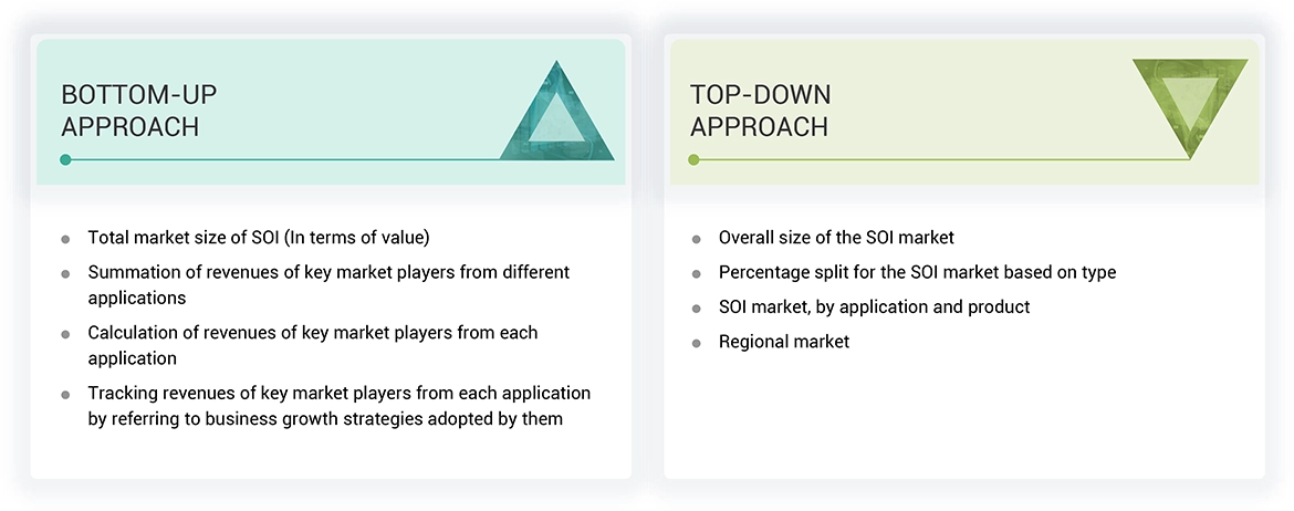
BOTTOM-UP APPROACH
-
17.2 FIGURE 2 SECONDARY AND PRIMARY RESEARCH
TOP-DOWN APPROACH
-
17.3 FIGURE 3 BOTTOM-UP APPROACH
MARKET SIZE ESTIMATION METHODOLOGY: SUPPLY-SIDE ANALYSIS (APPROACH 1)
-
17.4 FIGURE 4 TOP-DOWN APPROACH
MARKET SIZE ESTIMATION METHODOLOGY: SUPPLY-SIDE ANALYSIS (APPROACH 2)
-
17.5 FIGURE 5 MARKET SIZE ESTIMATION METHODOLOGY: SUPPLY-SIDE ANALYSIS (APPROACH 1)
MARKET SIZE ESTIMATION METHODOLOGY (APPROACH 3) – BOTTOM-UP (DEMAND SIDE): DEMAND FOR SOI WAFERS IN DIFFERENT APPLICATIONS
-
17.6 FIGURE 6 MARKET SIZE ESTIMATION METHODOLOGY: SUPPLY-SIDE ANALYSIS (APPROACH 2)
DATA TRIANGULATION
-
17.7 FIGURE 7 MARKET SIZE ESTIMATION METHODOLOGY (APPROACH 3) – BOTTOM-UP (DEMAND SIDE): DEMAND FOR SOI WAFERS IN DIFFERENT APPLICATIONS
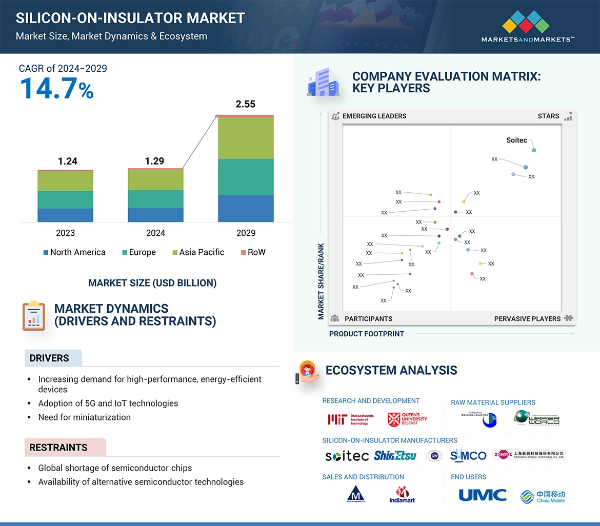
SILICON-ON-INSULATOR MARKET: GLOBAL SNAPSHOT, 2020–2029 (USD BILLION)
-
17.8 FIGURE 8 DATA TRIANGULATION
300MM SEGMENT TO LEAD MARKET DURING FORECAST PERIOD
-
17.9 FIGURE 9 SILICON-ON-INSULATOR MARKET: GLOBAL SNAPSHOT, 2020–2029 (USD BILLION)
RF-SOI SEGMENT TO LEAD MARKET DURING FORECAST PERIOD
-
17.10 FIGURE 10 300MM SEGMENT TO LEAD MARKET DURING FORECAST PERIOD
SMART CUT SOI SEGMENT TO DOMINATE MARKET DURING FORECAST PERIOD
-
17.11 FIGURE 11 RF-SOI SEGMENT TO LEAD MARKET DURING FORECAST PERIOD
MEMS DEVICES SEGMENT TO ACCOUNT FOR LARGEST MARKET BY 2029
-
17.12 FIGURE 12 SMART CUT SOI SEGMENT TO DOMINATE MARKET DURING FORECAST PERIOD
AUTOMOTIVE SEGMENT TO ACHIEVE HIGHEST GROWTH DURING FORECAST PERIOD
-
17.13 FIGURE 13 MEMS DEVICES SEGMENT TO ACCOUNT FOR LARGEST MARKET BY 2029
ASIA PACIFIC TO DOMINATE GLOBAL MARKET DURING FORECAST PERIOD
-
17.14 FIGURE 14 AUTOMOTIVE SEGMENT TO ACHIEVE HIGHEST GROWTH DURING FORECAST PERIOD
GROWING DEMAND FOR HIGH-PERFORMANCE, ENERGY-EFFICIENT DEVICES TO DRIVE MARKET GROWTH
-
17.15 FIGURE 15 ASIA PACIFIC TO DOMINATE GLOBAL MARKET DURING FORECAST PERIOD
CONSUMER ELECTRONICS SEGMENT TO ACCOUNT FOR LARGEST MARKET DURING FORECAST PERIOD
-
17.16 FIGURE 16 GROWING DEMAND FOR HIGH-PERFORMANCE, ENERGY-EFFICIENT DEVICES TO DRIVE MARKET GROWTH
RF-SOI SEGMENT TO ACCOUNT FOR LARGEST MARKET DURING FORECAST PERIOD
-
17.17 FIGURE 17 CONSUMER ELECTRONICS SEGMENT TO ACCOUNT FOR LARGEST MARKET DURING FORECAST PERIOD
SMART CUT SOI SEGMENT TO ACCOUNT FOR LARGEST MARKET DURING FORECAST PERIOD
-
17.18 FIGURE 18 RF-SOI SEGMENT TO ACCOUNT FOR LARGEST MARKET DURING FORECAST PERIOD
MEMS DEVICES SEGMENT TO LEAD MARKET DURING FORECAST PERIOD
-
17.19 FIGURE 19 SMART CUT SOI SEGMENT TO ACCOUNT FOR LARGEST MARKET DURING FORECAST PERIOD
300MM SEGMENT TO LEAD MARKET DURING FORECAST PERIOD
-
17.20 FIGURE 20 MEMS DEVICES SEGMENT TO LEAD MARKET DURING FORECAST PERIOD
CONSUMER ELECTRONICS SEGMENT AND CHINA TO ACCOUNT FOR SIGNIFICANT SHARE IN 2024
-
17.21 FIGURE 21 300MM SEGMENT TO LEAD MARKET DURING FORECAST PERIOD
SILICON-ON-INSULATOR MARKET: DRIVERS, RESTRAINTS, OPPORTUNITIES, AND CHALLENGES
-
17.22 FIGURE 22 CONSUMER ELECTRONICS SEGMENT AND CHINA TO ACCOUNT FOR SIGNIFICANT SHARE IN 2024
ELECTRIC CAR SALES, BY REGION, 2020–2024 (MILLION UNITS)
-
17.23 FIGURE 23 SILICON-ON-INSULATOR MARKET: DRIVERS, RESTRAINTS, OPPORTUNITIES, AND CHALLENGES
SILICON-ON-INSULATOR MARKET DRIVERS: IMPACT ANALYSIS
-
17.24 FIGURE 24 ELECTRIC CAR SALES, BY REGION, 2020–2024 (MILLION UNITS)
SILICON-ON-INSULATOR MARKET RESTRAINTS: IMPACT ANALYSIS
-
17.25 FIGURE 25 SILICON-ON-INSULATOR MARKET DRIVERS: IMPACT ANALYSIS
SILICON-ON-INSULATOR MARKET OPPORTUNITIES: IMPACT ANALYSIS
-
17.26 FIGURE 26 SILICON-ON-INSULATOR MARKET RESTRAINTS: IMPACT ANALYSIS
SILICON-ON-INSULATOR MARKET CHALLENGES: IMPACT ANALYSIS
-
17.27 FIGURE 27 SILICON-ON-INSULATOR MARKET OPPORTUNITIES: IMPACT ANALYSIS
VALUE CHAIN ANALYSIS
-
17.28 FIGURE 28 SILICON-ON-INSULATOR MARKET CHALLENGES: IMPACT ANALYSIS
SILICON-ON-INSULATOR MARKET: ECOSYSTEM
-
17.29 FIGURE 29 VALUE CHAIN ANALYSIS
INVESTMENT AND FUNDING SCENARIO, 2022–2024
-
17.30 FIGURE 30 SILICON-ON-INSULATOR MARKET: ECOSYSTEM
TRENDS/DISRUPTIONS IMPACTING CUSTOMER BUSINESS
-
17.31 FIGURE 31 INVESTMENT AND FUNDING SCENARIO, 2022–2024
AVERAGE SELLING PRICE TREND OF KEY PLAYERS FOR LESS THAN OR EQUAL TO 200MM SILICON-ON-INSULATORS
-
17.32 FIGURE 32 TRENDS/DISRUPTIONS IMPACTING CUSTOMER BUSINESS
AVERAGE SELLING PRICE TREND FOR WAFER SIZES, 2020–2023 (USD)
-
17.33 FIGURE 33 AVERAGE SELLING PRICE TREND OF KEY PLAYERS FOR LESS THAN OR EQUAL TO 200MM SILICON-ON-INSULATORS
AVERAGE SELLING PRICE TREND FOR SILICON-ON-INSULATORS, BY REGION, 2020–2023 (USD)
-
17.34 FIGURE 34 AVERAGE SELLING PRICE TREND FOR WAFER SIZES, 2020–2023 (USD)
SILICON-ON-INSULATOR MARKET: PORTER’S FIVE FORCES ANALYSIS
-
17.35 FIGURE 35 AVERAGE SELLING PRICE TREND FOR SILICON-ON-INSULATORS, BY REGION, 2020–2023 (USD)
INFLUENCE OF STAKEHOLDERS ON BUYING PROCESS FOR TOP THREE APPLICATIONS
-
17.36 FIGURE 36 SILICON-ON-INSULATOR MARKET: PORTER’S FIVE FORCES ANALYSIS
KEY BUYING CRITERIA FOR TOP THREE APPLICATIONS
-
17.37 FIGURE 37 INFLUENCE OF STAKEHOLDERS ON BUYING PROCESS FOR TOP THREE APPLICATIONS
IMPACT OF AI/GEN AI ON SILICON-ON-INSULATOR MARKET
-
17.38 FIGURE 38 KEY BUYING CRITERIA FOR TOP THREE APPLICATIONS
IMPORT DATA FOR HS CODE: 854690-COMPLIANT PRODUCTS, BY COUNTRY, 2019–2023 (USD MILLION)
-
17.39 FIGURE 39 IMPACT OF AI/GEN AI ON SILICON-ON-INSULATOR MARKET
EXPORT DATA FOR HS CODE: 854690-COMPLIANT PRODUCTS, BY COUNTRY, 2019–2023 (USD MILLION)
-
17.40 FIGURE 40 IMPORT DATA FOR HS CODE: 854690-COMPLIANT PRODUCTS, BY COUNTRY, 2019–2023 (USD MILLION)
NUMBER OF PATENTS GRANTED FOR SILICON-ON-INSULATOR MARKET, 2013–2023
-
17.41 FIGURE 41 EXPORT DATA FOR HS CODE: 854690-COMPLIANT PRODUCTS, BY COUNTRY, 2019–2023 (USD MILLION)
300MM SEGMENT TO DOMINATE MARKET DURING FORECAST PERIOD
-
17.42 FIGURE 42 NUMBER OF PATENTS GRANTED FOR SILICON-ON-INSULATOR MARKET, 2013–2023
RF-SOI SEGMENT TO ACCOUNT FOR LARGEST MARKET DURING FORECAST PERIOD
-
17.43 FIGURE 43 300MM SEGMENT TO DOMINATE MARKET DURING FORECAST PERIOD
SMART CUT SOI SEGMENT TO DOMINATE MARKET DURING FORECAST PERIOD
-
17.44 FIGURE 44 RF-SOI SEGMENT TO ACCOUNT FOR LARGEST MARKET DURING FORECAST PERIOD
MEMS DEVICES SEGMENT TO LEAD MARKET DURING FORECAST PERIOD
-
17.45 FIGURE 45 SMART CUT SOI SEGMENT TO DOMINATE MARKET DURING FORECAST PERIOD
AUTOMOTIVE SEGMENT TO REGISTER HIGHEST CAGR DURING FORECAST PERIOD
-
17.46 FIGURE 46 MEMS DEVICES SEGMENT TO LEAD MARKET DURING FORECAST PERIOD
CHINA TO GROW AT HIGHEST CAGR DURING FORECAST PERIOD
-
17.47 FIGURE 47 AUTOMOTIVE SEGMENT TO REGISTER HIGHEST CAGR DURING FORECAST PERIOD
NORTH AMERICA: SILICON-ON-INSULATOR MARKET SNAPSHOT
-
17.48 FIGURE 48 CHINA TO GROW AT HIGHEST CAGR DURING FORECAST PERIOD
EUROPE: SILICON-ON-INSULATOR MARKET SNAPSHOT
-
17.49 FIGURE 49 NORTH AMERICA: SILICON-ON-INSULATOR MARKET SNAPSHOT
ASIA PACIFIC: SILICON-ON-INSULATOR MARKET SNAPSHOT
-
17.50 FIGURE 50 EUROPE: SILICON-ON-INSULATOR MARKET SNAPSHOT
MARKET SHARE ANALYSIS, 2023
-
17.51 FIGURE 51 ASIA PACIFIC: SILICON-ON-INSULATOR MARKET SNAPSHOT
REVENUE ANALYSIS OF KEY PLAYERS, 2019–2023 (USD MILLION)
-
17.52 FIGURE 52 MARKET SHARE ANALYSIS, 2023
COMPANY VALUATION
-
17.53 FIGURE 53 REVENUE ANALYSIS OF KEY PLAYERS, 2019–2023 (USD MILLION)
FINANCIAL METRICS
-
17.54 FIGURE 54 COMPANY VALUATION
SILICON-ON-INSULATOR MARKET: COMPANY EVALUATION MATRIX (KEY PLAYERS), 2023
-
17.55 FIGURE 55 FINANCIAL METRICS
SILICON-ON-INSULATOR MARKET: COMPANY FOOTPRINT
-
17.56 FIGURE 56 SILICON-ON-INSULATOR MARKET: COMPANY EVALUATION MATRIX (KEY PLAYERS), 2023
SILICON-ON-INSULATOR MARKET: COMPANY EVALUATION MATRIX (STARTUPS/SMES), 2023
-
17.57 FIGURE 57 SILICON-ON-INSULATOR MARKET: COMPANY FOOTPRINT
BRAND/PRODUCT COMPARISON
-
17.58 FIGURE 58 SILICON-ON-INSULATOR MARKET: COMPANY EVALUATION MATRIX (STARTUPS/SMES), 2023
SOITEC: COMPANY SNAPSHOT
-
17.59 FIGURE 59 BRAND/PRODUCT COMPARISON
SHIN-ETSU CHEMICAL CO., LTD.: COMPANY SNAPSHOT
-
17.60 FIGURE 60 SOITEC: COMPANY SNAPSHOT
GLOBALWAFERS: COMPANY SNAPSHOT
-
17.61 FIGURE 61 SHIN-ETSU CHEMICAL CO., LTD.: COMPANY SNAPSHOT
SUMCO CORPORATION: COMPANY SNAPSHOT
-
17.62 FIGURE 62 GLOBALWAFERS: COMPANY SNAPSHOT
GLOBALFOUNDRIES: COMPANY SNAPSHOT
-
17.63 FIGURE 63 SUMCO CORPORATION: COMPANY SNAPSHOT
STMICROELECTRONICS: COMPANY SNAPSHOT
-
17.64 FIGURE 64 GLOBALFOUNDRIES: COMPANY SNAPSHOT
TOWER SEMICONDUCTOR: COMPANY SNAPSHOT
-
FIGURE 65 STMICROELECTRONICS: COMPANY SNAPSHOT
-
FIGURE 66 TOWER SEMICONDUCTOR: COMPANY SNAPSHOT


 HIGHEST CAGR MARKET IN 2024
 CHINA FASTEST GROWING MARKET IN THE REGION
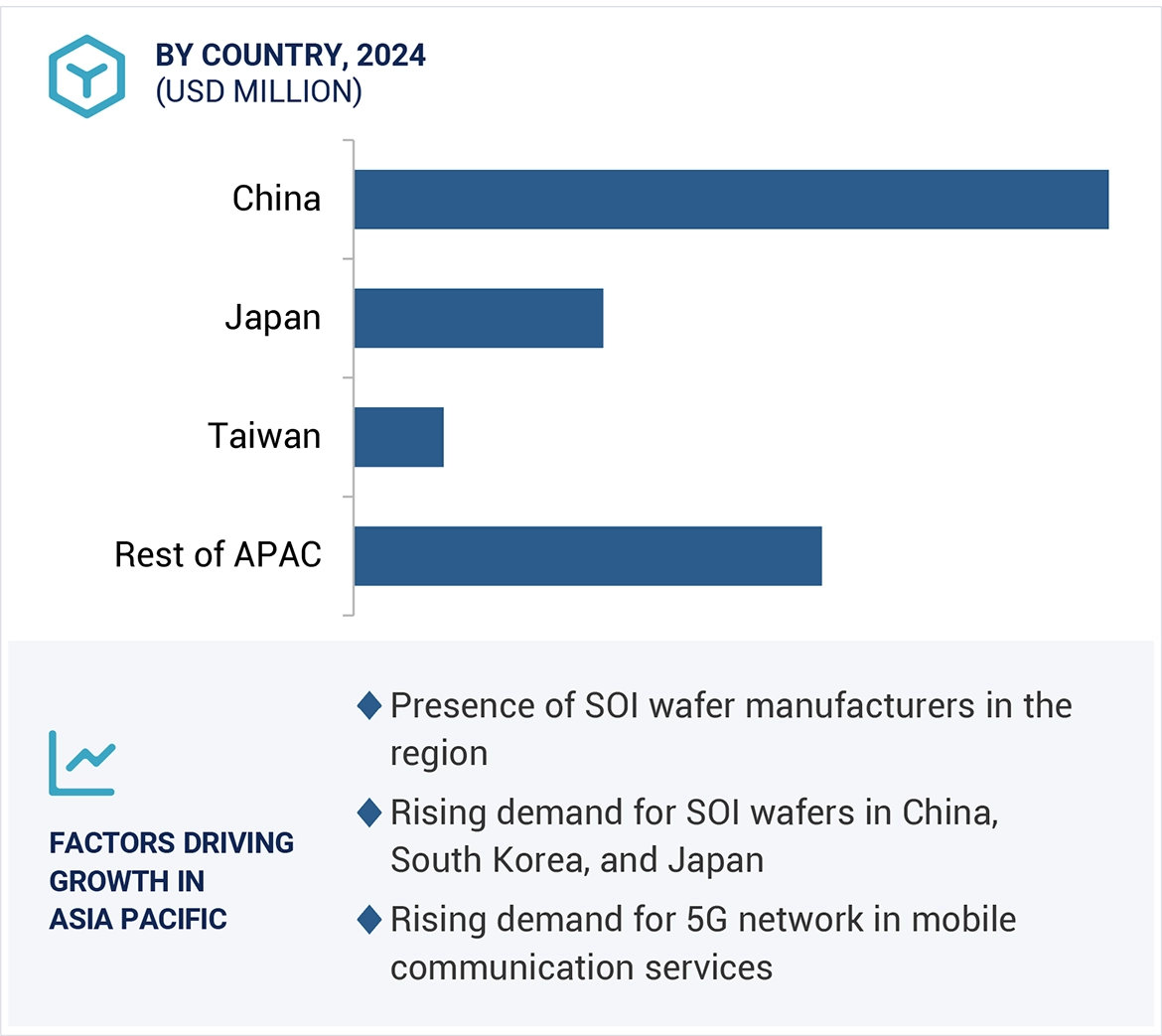


Angelina
Sep, 2011
Need following information 1. 200mm prime wafer historical pricing & future pricing trends per wafer type : Epi wafer (p/p-, p/p+ type), polished wafer (p type), annealed wafer, monitor wafer (N type), SOI wafer 2. World wide top 10 silicon supplier / manufacturer status / new product launches..
Tien-Hsi
May, 2015
If you would like to provide the report with great discount for the education purpose that lets future engineers recognize SOI's key role in microelectronic industry, please let me know. .
Jeongseok
Sep, 2019
Hello, I just wonder if there is any benefit on Automotive OEM manufacturers by using specific IC which is made on SOI wafer. I fully understand some benefit on IC maker side and Tier1 or 2 side and same for OEM. But need to gain more information..
Arthur
Nov, 2010
I would like to know the market size and growth of SOI semiconductor as well as the major product applications and TAM..
Shefali
Sep, 2019
We had purchased the report a few months back. We have some queries on the market and would like to speak to the analyst. Kindly connect with me as soon as possible..
Brian
Nov, 2011
Hi, we need sections 1, 2, 4, and 7 for our Technology Management Program class on microchips. .
jean
Sep, 2018
I see a huge difference between your 2018 report and the one of April 2017 on the same subject (SOI); in particular the alternative technologies to smart cut like Eltran. Could you explain ?.
Rajappan
Sep, 2019
Interested in understanding if you cover the market share of RF SOI foundries (e.g., what percent of an RF SOI foundry is used by company X vs Y vs Z).
Elisabeth
Jun, 2019
Hi, I am wondering if you make discounts for start-ups as we are interested in your report. .
CY
May, 2019
Need help for our SOI technology development study. Requirement is for market size by SOI type, application and wafer size..
Terence
Mar, 2014
Please let me know more about this report. My focus is to understand the RFSOI TAM and who are the chip makers (RFMD/Skyworks/etc.) and their potential growth beyond 2019. .