
Atomic Force Microscopy Market Size, Share & Trends

Atomic Force Microscopy Market Size, Share & Trends by Offering (AFMs, Probes, Software), Grade (Industrial, Research), Application (Semiconductors & Electronics, Material Science & Nanotechnology, Life Sciences & Biomedical) and Region - Global Forecast to 2030


ATOMIC FORCE MICROSCOPY MARKET SIZE, SHARE & TRENDS
According to Marketsandmarkets The global atomic force microscopy market size is projected to grow from USD 541.8 million in 2025 to USD 762.2 billion by 2030 growing at a CAGR of 7.1%. The ongoing advancements in high-speed and high-resolution imaging technologies and the integration of multifunctional capabilities are pivotal drivers of growth in the atomic force microscopy (AFM) market.
MARKET SCOPE
| REPORT METRIC | DETAILS |
|---|---|
| Market Size in 2025 (Value) | USD 541.8 Million |
| Market Forecast in 2030 (Value) | USD 762.2 Million |
| Growth Rate | CAGR of 7.1% from 2025-2030 |
| Years Considered | 2021-2030 |
| Base Year | 2024 |
| Forecast Period | 2025-2030 |
| Units Considered | Value (USD Million) |
| Report Coverage | Revenue forecast, company ranking, competitive landscape, growth factors, and trends |
| Top Companies |
|
| Growth Driver |
|
| Segments Covered |
|
| Regions Covered | North America, Asia Pacific, Europe, RoW |
KEY TAKEAWAYS
-
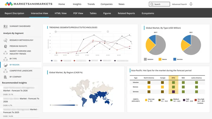
By RegionAsia Pacific atomic force microscopy market accounted for a 47.3% revenue share in 2024.
-
By GradeBy grade, the industrial segment is expected to register the highest CAGR of 7.5%.
-
By ApplicationBy application, the semiconductors & electronics segment is projected to grow at the fastest rate from 2025 to 2030.
-
Competitive LandscapeGeTec Micrscopy GmbH, Labtrom Equipment Ltd., and Molecular Vista among others, have distinguished themselves among startups and SMEs by securing strong footholds in specialized niche areas, underscoring their potential as emerging market leaders
The escalating utilization of Atmoic force microscope (AFM) for subsurface imaging in semiconductor metrology and its burgeoning application in cellular biomechanics and nano-biological research are creating new commercial prospects across both industrial and academic sectors. These advancements are broadening the applicability of AFM within various rapidly growing fields, including materials science, electronics, and life sciences.

Source: Secondary Research, Interviews with Experts, MarketsandMarkets Analysis
TRENDS & DISRUPTIONS IMPACTING CUSTOMERS' CUSTOMERS
The Atomic Force Microscope market is transitioning from primarily research-focused applications toward broader industrial and high-throughput use. Growth is being driven by advances in automation, faster scanning technologies, AI-assisted image analysis, and integration with other microscopy and metrology platforms. These developments are expanding AFM adoption beyond academia into semiconductor process control, battery and materials R&D, and life-science applications, where precise nanoscale characterization directly supports innovation and quality assurance.

Source: Secondary Research, Interviews with Experts, MarketsandMarkets Analysis
MARKET DYNAMICS
Level
-
Need for nanoscale precision in semiconductor manufacturing.

-
High investments in nanotechnology.

Level
-
Damage to samples due to contact-mode atomic force microscopy.

-
Critical sample preparation requirements.

Level
-
Emerging applications from basic imaging to multi-modal analysis due to technological advancements.

-
Growing investments in OLED panel production globally.

Level
-
High-throughput challenges due to surface coverage and speed limitations.

Source: Secondary Research, Interviews with Experts, MarketsandMarkets Analysis
Driver: High investments in nanotechnology.
Rising investments in nanotechnology research continue to be a significant driver for the atomic force microscopy market. Recent increases in funding from both public and private sectors are strengthening the demand for high-precision tools capable of nanoscale characterization. AFM technology plays a crucial role in enabling researchers to visualize, manipulate, and analyze structures at the atomic and molecular level. These capabilities are especially critical in developing advanced materials, nanoelectronics, drug delivery systems, and biosensors.
Restraint: Damage to samples due to contact-mode atomic force microscopy.
Contact-mode AFM is one of the earliest and most common techniques for high-resolution surface topography. In this mode, the tip remains in continuous contact with the sample surface, controlled by a feedback loop operating in either constant-force or constant-height mode. While effective, this continuous contact often generates strong lateral and adhesive forces that can damage or distort soft materials such as polymers, biological tissues, or macromolecules. Such forces may displace fragile structures and create imaging artifacts, reducing data accuracy and compromising sample integrity.
Opportunity: Emerging applications from basic imaging to multi-modal analysis due to technological advancements.
Innovations such as high-speed scanning, improved force sensitivity, and multimodal imaging capabilities have substantially expanded the operational scope of AFMs beyond traditional surface topography analysis. These developments allow real-time monitoring of dynamic nanoscale processes, offering critical insights into advanced materials research, molecular biology, and semiconductor manufacturing. Furthermore, integrating artificial intelligence and machine learning in AFM systems enables automated image analysis, defect detection, and adaptive scanning protocols, which significantly enhance throughput and data accuracy.
Challenge: High-throughput challenges due to surface coverage and speed limitations.
AFM offers exceptional nanoscale resolution but is limited by its small scan area, typically only tens of micrometers. While ideal for detailed surface analysis, this restricts its use in large-area inspections such as semiconductor wafers, flexible displays, and composite materials. Scanning extensive surfaces requires stitching multiple small images, which is time-consuming and can introduce alignment errors, reducing efficiency for industrial applications.
Atomic Force Microscopy Market: COMMERCIAL USE CASES ACROSS INDUSTRIES
| COMPANY | USE CASE DESCRIPTION | BENEFITS |
|---|---|---|
 |
Bruker offers high-resolution AFMs for nanomechanical, electrical, and chemical characterization in materials science, semiconductors, and life sciences. | High spatial resolution, versatile imaging modes, quantitative nanomechanical mapping, and reliable performance for both research and industrial QA/QC. |
 |
Hitachi AFMs are integrated with electron microscopy systems to provide correlative surface and structural analysis at the nanoscale. | Enables combined AFM–SEM workflows; precise 3D surface mapping; improved productivity in nanomaterial and semiconductor analysis. |
 |
Provides AFMs integrated into cryogenic and magnetic environments for advanced materials and quantum research applications. | Allows AFM imaging under extreme conditions (low temperature, high magnetic fields); supports nanoscale studies of superconductors and 2D materials |
 |
Offers AFMs optimized for high-speed, automated, and non-contact nanoscale imaging used in semiconductor, materials, and bio research. | High throughput with automated measurements; true non-contact mode preserves samples; exceptional accuracy and repeatability. |
 |
Develops AFM-based metrology systems for semiconductor wafer surface analysis and defect inspection. | Enables inline process control; high-resolution 3D topography for thin films and surfaces; improved yield and reliability in semiconductor manufacturing. |
Logos and trademarks shown above are the property of their respective owners. Their use here is for informational and illustrative purposes only.
MARKET ECOSYSTEM
The Atomic Force Microscopy ecosystem brings together a global network of manufacturers, distributors, and end users driving nanoscale innovation. Leading instrument makers such as Park Systems, Bruker, and Hitachi collaborate with specialized distributors and analytical partners to deliver advanced AFM technologies to research institutions and industrial customers worldwide. This integrated value chain supports applications across academia, semiconductors, materials science, biotechnology, and nanotechnology enabling precise surface characterization and accelerating breakthroughs from research to real-world manufacturing.

Logos and trademarks shown above are the property of their respective owners. Their use here is for informational and illustrative purposes only.
MARKET SEGMENTS

Source: Secondary Research, Interviews with Experts, MarketsandMarkets Analysis
Atomic Force Microscopy Market, By Grade
The industrial segment is expected to hold a larger share of the atomic force microscope (AFM) market during forecast period due to its widespread application in high-precision manufacturing sectors, such as semiconductors, materials science, and nanotechnology. AFM plays a crucial role in quality control, process optimization, and failure analysis in industrial environments by enabling detailed surface characterization and nanoscale measurements. Industries use AFM to inspect surface topography, detect defects, and evaluate mechanical properties of materials, all of which are vital for maintaining stringent production standards.
Atomic Force Microscopy Market, By Application
The semiconductors and electronics segment is expected to hold the largest share of the atomic force microscopy market due to its critical need for nanoscale surface characterization and defect analysis during device fabrication. Atomic force microscopes are extensively used in semiconductor manufacturing for inspecting thin films, measuring feature dimensions, detecting defects, and assessing line-edge roughness at sub-nanometer resolution. As device architectures continue to shrink with the advancement of FinFETs, 3D NAND, and chiplet-based designs, the demand for precise metrology tools, such as AFMs, has intensified.
REGION
Asia Pacific to be fastest-growing region in global atomic force microscopy market during forecast period
The Asia Pacific atomic force microscopy market is expected to register the highest CAGR during the forecast period, due to a strong combination of industrial capabilities, research infrastructure, and regional innovation policies. The region is a global hub for semiconductor and electronics manufacturing, with countries such as Japan, South Korea, and Taiwan relying extensively on AFM systems for nanoscale inspection, defect analysis, and quality control in microchip production. India and Singapore are also emerging as important contributors, with increasing investments in nanotechnology, biotechnology, and advanced materials research.

Atomic Force Microscopy Market: COMPANY EVALUATION MATRIX
In the atomic force microscopy market matrix, Park System (Star) leads with a strong market share the global leader in the atomic force microscope (AFM) market, renowned for its cutting-edge nanotechnology solutions and precision instrumentation. Semilab, Inc. (Emerging Leader) is gaining visibilityin the semiconductor metrology and inspection sector, rapidly gaining recognition for its advanced, high-performance solutions that drive efficiency and insight in materials characterization.

Source: Secondary Research, Interviews with Experts, MarketsandMarkets Analysis
KEY MARKET PLAYERS
WHAT IS IN IT FOR YOU: Atomic Force Microscopy Market REPORT CONTENT GUIDE

DELIVERED CUSTOMIZATIONS
We have successfully delivered the following deep-dive customizations:
| CLIENT REQUEST | CUSTOMIZATION DELIVERED | VALUE ADDS |
|---|---|---|
| CLIENT REQUEST | CUSTOMIZATION DELIVERED | VALUE ADDS |
| Leading Semiconductor OEM |
|
|
| AFM Instrument Manufacturer |
|
|
| Tip & Cantilever Supplier |
|
|
| Raw Material Supplier |
|
|
RECENT DEVELOPMENTS
- May 2025 : Oxford Instruments (UK) launched the Jupiter Discovery Atomic Force Microscope (AFM). This advanced AFM is designed for large-sample applications and provides high-resolution imaging, reliable repeatability, and enhanced throughput. Its intuitive interface and accessible design enable researchers across academic and industrial sectors, including those with limited training, to conduct high-precision measurements.
- February 2025 : Park Systems (South Korea) launched its expanded FX Large Sample AFM series at SEMICON Korea 2025. The company introduced the Park FX300 for advanced 300 mm wafer analysis. Additionally, Park Systems unveiled the Park FX200 IR and FX300 IR, which incorporate infrared (IR) spectroscopy, further advancing the capabilities of large-sample AFM technology.
- December 2024 : Bruker (US) launched the Dimension Nexus atomic force microscope, a compact and upgradable system featuring the latest NanoScope 6 controller and PeakForce Tapping technology. This new addition to the Dimension AFM line is designed to meet the needs of expanding laboratories and multi-user facilities.
Table of Contents
 Exclusive indicates content/data unique to MarketsandMarkets and not available with any competitors.
Methodology
The study involved major activities in estimating the atomic force microscopy market size. Exhaustive secondary research was done to collect information on the market. The next step was to validate these findings, assumptions, and sizing with industry experts across the value chain using primary research. Different approaches, such as top-down and bottom-up, were employed to estimate the total market size. After that, the market breakup and data triangulation procedures were used to estimate the market size of the segments and subsegments of the atomic force microscopy market.
Secondary Research
The market size for atomic force microscopy offerings (atomic force microscopes, probes, and software) was determined by secondary data available through paid and unpaid sources, analyzing the product portfolios of the major companies in the ecosystem, and rating the companies by their performance and quality. Various sources were referred to in the secondary research process to identify and collect information for this study. The secondary sources include annual reports, press releases, investor presentations of companies, white papers, journals, certified publications, and articles from recognized authors, directories, and databases. In the secondary research process, various secondary sources were referred to identify and collect information related to the study. Secondary sources included annual reports, press releases, investor presentations of vendors, forums, certified publications, and whitepapers. The secondary research was used to obtain critical information on the industry's value chain, the total pool of key players, market classification, and segmentation from the market and technology-oriented perspectives.
Primary Research
Extensive primary research has been conducted after understanding and analyzing the current scenario of the atomic force microscopy market through secondary research. Several primary interviews have been conducted with the key opinion leaders from the demand and supply sides across four main regions—North America, Europe, Asia Pacific, and Rest of the World (RoW). Approximately 30% of the primary interviews were conducted with the demand-side respondents, while approximately 70% were conducted with the supply-side respondents. The primary data has been collected through questionnaires, emails, and telephone interviews.
After interacting with industry experts, brief sessions were conducted with highly experienced independent consultants to reinforce the findings from our primary research. This, along with the in-house subject-matter experts’ opinions, has led us to the findings as described in the remainder of this report. The breakdown of primary respondents is as follows:

Note: The 3 tiers of companies have been defined based on their total revenue as of 2024; tier 1: revenue greater than USD 100 million, tier 2: revenue between USD 50 million and USD 100 million, and tier 3: revenue less than USD 50 million. Others include sales consultants and marketing managers.
To know about the assumptions considered for the study, download the pdf brochure
Market Size Estimation
Both top-down and bottom-up approaches were used to estimate and validate the total size of the atomic force microscopy market. These methods were also used extensively to estimate the size of various subsegments in the market. The research methodology used to estimate the market size includes the following:
Atomic Force Microscopy Market : Top-Down and Bottom-Up Approach

Data Triangulation
The market was split into several segments and subsegments after arriving at the overall market size using the market size estimation processes explained above. Wherever applicable, the data triangulation and market breakdown procedures were employed to complete the overall market engineering process and arrive at the exact statistics of each market segment and subsegment. The data was triangulated by studying various factors and trends from the demand and supply sides.
Market Definition
An atomic force microscope (AFM) is a precision instrument designed to examine surfaces at the nanometer and atomic scales. It uses a sharp probe tip that moves across the sample in a raster pattern to gather detailed information about the surface properties. The AFM provides much higher resolution than traditional optical microscopes, as the diffraction of light does not limit it. Data is collected through direct contact with the surface or close-range interaction between the probe and the sample. The microscope includes piezoelectric elements, which are materials that respond to electrical signals by producing very small and precise mechanical movements, allowing for highly accurate scanning.
Key Stakeholders
- Pharmaceuticals and biotechnology industries
- Semiconductor and materials industries
- Academic and research institutes
- Pathological laboratories
- Hospitals
- Medical device suppliers
- Market research and consulting firms
Report Objectives
- To describe and forecast the size of the atomic force microscopy market, by offering, grade, application, and region, in terms of value
- To describe and forecast the size of the market across four main regions, namely, North America, Europe, Asia Pacific, and Rest of the World, in terms of value
- To provide detailed information regarding drivers, restraints, opportunities, and challenges influencing the growth of the market
- To strategically analyze micromarkets with respect to individual growth trends, prospects, and contributions to the total market
- To analyze opportunities in the market for various stakeholders by identifying high-growth segments of the atomic force microscopy market
- To benchmark players within the market using the proprietary "Competitive Leadership Mapping" framework, which analyzes market players on various parameters within the broad categories of business strategy excellence and strength of product portfolio
- To strategically profile key players and comprehensively analyze their market position in terms of ranking and core competencies, along with detailing the competitive landscape of the market
- To analyze competitive developments such as acquisitions, product launches and developments, and research and development in the atomic force microscopy market
Available customizations:
With the given market data, MarketsandMarkets offers customizations according to the specific requirements of companies. The following customization options are available for the report:
- Detailed analysis and profiling of additional market players based on various blocks of the supply chain
Key Questions Addressed by the Report
1
What is the current size of the Atomic Force Microscopy Market?
2
What is the expected growth rate of the AFM market?
3
What are the major growth drivers of the AFM market?
4
Which application segment is growing the fastest?
5
Which region dominates the Atomic Force Microscopy market?
6
What are the latest trends in the AFM market?
7
Which companies are leading the Atomic Force Microscopy market?
8
Which end-use industries are driving AFM adoption?
9
Which market segment is expected to grow fastest by offering?
10
What opportunities exist in the AFM market through 2030?
Need a Tailored Report?
Customize this report to your needs
Get 10% FREE Customization
Customize This ReportPersonalize This Research
- Triangulate with your Own Data
- Get Data as per your Format and Definition
- Gain a Deeper Dive on a Specific Application, Geography, Customer or Competitor
- Any level of Personalization
Let Us Help You
- What are the Known and Unknown Adjacencies Impacting the Atomic Force Microscopy Market
- What will your New Revenue Sources be?
- Who will be your Top Customer; what will make them switch?
- Defend your Market Share or Win Competitors
- Get a Scorecard for Target Partners

Custom Market Research Services
We Will Customise The Research For You, In Case The Report Listed Above Does Not Meet With Your Requirements
Get 10% Free CustomisationTESTIMONIALS

Tetsuya Ohhira
Business Development Manager-Technology Business
Nikon Corporation,
Leading Japanese MNC specializing in optics and imaging productswww.nikon.com
MarketsandMarkets™ response
is quick. Their attitude is flexible and positive. Analyst Insights are globally considered and
significant. Client Services quickly respond to our inquiry and demand. Their wide range of global
surveys help us make our strategic plan.
We hope Knowledge Store will be easier to search
for a report.
VP - Marketing & Business Development
Leading Provider of Process Control Solutions
We engaged with MarketsandMarkets on a study to perform an analysis and recommend a Go-To-Market strategy for metrology and process control in the semiconductor market. The study was tailored to our targets and needs with well-defined milestones. Our overall experience with the MarketsandMarkets team was very good throughout the project in all aspects including the analysis methodologies used, the quality and depth of primary and secondary data sets, the professionalism and flexibility of the team and the ability to meet the target schedule and milestones. We want to thank MarketsandMarkets team for a job well done.


Growth opportunities and latent adjacency in Atomic Force Microscopy Market