
China MEMS Packaging Substrates Market (2025-2030)

The China MEMS Packaging Substrates Market was valued at $467.1 Million in 2025 and projected to reach to $646.4 Million by 2030, representing a compound annual growth rate of 6.7%. China's MEMS packaging substrates market is poised for sustained growth driven by the country's dominance in semiconductor manufacturing and rapid expansion of consumer electronics production.


| Market Size in | USD 26.32 MN |
| Market Forecast in | |
| CAGR | |
| Forecast Period | |
| Units Considered | Value (USD MN) |
China MEMS Packaging Substrates Market Trends and Insights
- China's dominance in semiconductor manufacturing and consumer electronics production drives substantial demand for advanced MEMS packaging solutions across automotive, industrial, and consumer applications.
- The country's strategic investments in microelectronics infrastructure and growing adoption of IoT and 5G technologies position China as a critical hub for MEMS substrate innovation and production. China's market growth is underpinned by increasing miniaturization requirements in smartphones, wearables, and automotive sensors, where MEMS packaging substrates play a vital role in device performance and reliability.
- China's robust supply chain ecosystem and cost-competitive manufacturing capabilities enable rapid scaling of MEMS packaging solutions.
- Between 2025 and 2030, China is expected to capture significant market share as domestic and international manufacturers expand production capacity to meet rising demand from both domestic consumption and export markets..
Key Market Statistics
- CAGR (2025-2030) 6.7% CAGR
- Market Size, 2025 ~USD 467.1 Million
- Forecast, 2030 ~USD 646.4 Million
- Country China
China MEMS Packaging Substrates Market Overview
Market Valuation & Growth :
China's MEMS packaging substrates market is valued at $467.1 million in 2025 and is projected to reach $646.4 million by 2030, representing a robust 6.7% CAGR, outpacing the global growth rate of 6.1%.
Manufacturing Leadership :
China's position as the world's leading semiconductor manufacturing hub drives exceptional demand for advanced MEMS packaging solutions, with domestic production capacity supporting both domestic consumption and global supply chains.
Application Diversification :
Strong growth across automotive, industrial, and consumer electronics sectors in China creates multiple revenue streams for MEMS packaging substrate suppliers, with automotive applications showing particularly robust expansion.
Technology Integration :
Increasing adoption of advanced packaging technologies in Chinese consumer electronics and IoT devices is accelerating demand for high-performance MEMS substrates with enhanced thermal and electrical properties.
China MEMS Packaging Substrates Market Dynamics
- The 6.7% CAGR reflects strong domestic demand from automotive electrification, industrial automation, and 5G infrastructure development.
- Government initiatives supporting semiconductor self-sufficiency and advanced manufacturing capabilities are expected to further bolster market expansion through 2030. The competitive landscape in China is intensifying as local manufacturers invest in advanced packaging technologies to reduce import dependency.
- Rising consumer demand for smart devices, wearables, and IoT applications continues to fuel substrate consumption.
- Strategic partnerships between Chinese semiconductor companies and packaging substrate manufacturers are creating new growth opportunities, positioning China as a critical hub for MEMS packaging innovation and production..
Market Ecosystem
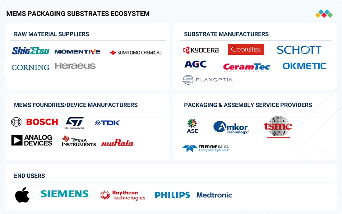
MEMS Packaging Substrates Market: COMMERCIAL USE CASES ACROSS INDUSTRIES
| COMPANY | USE CASE DESCRIPTION | BENEFITS |
|---|---|---|
 |
Ceramic and glass-ceramic substrates used in automotive MEMS pressure sensors, accelerometers, and gyroscopes for advanced driver-assistance systems (ADAS) and electric vehicles | Enables high reliability under thermal and mechanical stress, supports miniaturization, and ensures long-term stability for safety-critical automotive applications |
 |
Alumina and AlN substrates supporting MEMS-based flow, pressure, and vibration sensors in industrial automation and aerospace systems | Offers superior heat dissipation, electrical insulation, and mechanical durability, extending device lifespan in extreme conditions |
 |
Ceramic packaging substrates for MEMS sensors used in medical diagnostics equipment and laboratory instrumentation | Provides biocompatibility, chemical resistance, and precision sealing for reliable sensor performance in sterile and high-sensitivity environments |
 |
Glass substrates and Through-Glass Via (TGV) wafers integrated into MEMS optical sensors and LiDAR modules for consumer electronics and autonomous vehicles | Ensures optical clarity, flatness, and fine-pitch interconnects, improving signal quality and accuracy in imaging and depth-sensing applications |
 |
Specialty glass substrates (BOROFLOAT®, FLEXINITY®) used in MEMS microphones and environmental sensors for smartphones and wearables | Provides miniaturization capability, excellent dimensional stability, and acoustic transparency, enhancing performance and device slimness |
Logos and trademarks shown above are the property of their respective owners. Their use here is for informational and illustrative purposes only.
Related Ecosystem
Electrical System And Components
Key Takeaways
- China's MEMS packaging substrates market is valued at $467.1 million in 2025 and will grow to $646.4 million by 2030 at a 6.7% CAGR.
- China's semiconductor manufacturing leadership and consumer electronics dominance create strong demand drivers for advanced MEMS packaging solutions.
- China's investments in 5G, IoT, and automotive electrification are accelerating adoption of MEMS-based sensors requiring specialized packaging substrates.
- China's cost-competitive manufacturing and integrated supply chain position the country as a global leader in MEMS packaging substrate production and innovation.
MEMS Packaging Substrates Market Report Scope
| Report Metric | Details |
|---|---|
| Base Year | 2025 |
| Fastest Growing Segment | TELECOM (Vertical) |
| Forecast Period | 2025–2030 |
| Growth Rate | CAGR of 6.1% from 2025 to 2030 |
| Largest Segment | SENSORS (Application) |
| Market Size Base Year (Billions) | ~USD 2.4 (2025) |
| Revenue Forecast (Billions) | ~USD 3.23 (2030) |
| Segments Covered | Substrate Type, Application, Type, Vertical |
China MEMS Packaging Substrates Market Report Segmentation
4 segment dimensions are covered across the global market.
By Substrate Type
- Ceramic
- Glass
- Organic
- Silicon
By Application
- Actuators
- Sensors
By Type
- Environmental Sensors
- Inertial Sensors
- Inkjet Head
- Microfluidic
- Microphones
- Microspeaker
- Optical
- Optical Sensors
- Other Sensor Types
- Pressure Sensors
- Radio Frequency
By Vertical
- Aerospace
- Automotive
- Consumer Electronics
- Defense
- Healthcare
- Industrial
- Telecom
CHINA: MEMS PACKAGING SUBSTRATES MARKET, BY VERTICAL, 2025–2030
| Segment | 2025 | 2026 | 2027 | 2028 | 2029 | 2030 | CAGR (%) |
|---|---|---|---|---|---|---|---|
| AEROSPACE | 15.8 | 16.8 | 17.8 | 18.8 | 19.9 | 21 | 5.9 |
| AUTOMOTIVE | 86.2 | 92.7 | 99.4 | 106.2 | 113.4 | 120.8 | 7 |
| CONSUMER ELECTRONICS | 227.6 | 243.1 | 258.6 | 274.3 | 290.3 | 306.9 | 6.2 |
| DEFENSE | 34.7 | 37.6 | 40.6 | 43.7 | 47 | 50.4 | 7.7 |
| HEALTHCARE | 41.7 | 45 | 48.4 | 51.8 | 55.3 | 59.1 | 7.2 |
| INDUSTRIAL | 49.7 | 53.5 | 57.4 | 61.4 | 65.5 | 69.8 | 7 |
| TELECOM | 11.3 | 12.6 | 13.9 | 15.3 | 16.7 | 18.4 | 10.1 |
| TOTAL | 467.1 | 501.4 | 536.1 | 571.5 | 608.1 | 646.4 | 6.7 |
Target Audience
- Chinese Semiconductor Manufacturers : Need detailed market insights to optimize MEMS packaging substrate sourcing, evaluate domestic supplier capabilities, and plan production capacity investments aligned with market growth projections.
- Automotive OEMs & Suppliers : Require China-specific data on MEMS packaging demand for automotive applications, including sensor integration trends, EV electrification impacts, and supplier qualification requirements in the Chinese market.
- Packaging Substrate Producers : Seek competitive intelligence on China's market size, growth rates, and application segments to inform capacity planning, technology investments, and market entry or expansion strategies in this critical region.
- Electronics & IoT Device Manufacturers : Need market forecasts and application trends specific to China to guide MEMS component sourcing decisions, cost optimization strategies, and product development aligned with domestic consumer demand.
- Investment & Strategy Consultants : Require comprehensive China market data to support M&A analysis, investment thesis development, and strategic recommendations for clients targeting the high-growth MEMS packaging substrates sector.
Key Companies in the China MEMS Packaging Substrates Market
| Company | HQ | Ownership | Strongest segments |
|---|---|---|---|
| SHIN-ETSU CHEMICAL CO., LTD. | Japan | Public Company | Semiconductor silicon and electronic materials,PVC and chlor-alkali (polyvinyl chloride, caustic soda, methanol, chloromethanes),Silicones and silicon-related functional materials, |
| KYOCERA CORPORATION | Japan | Public Company | Core Components (fine ceramics, packages, optical, medical),Electronic Components (sensors, capacitors, crystals, connectors, power devices),Solutions (cutting tools, printers, MFPs, ICT, smart energy, terminals), |
| AGC INC. | United States | Public Company | High-horsepower and row-crop tractors,Utility and compact tractors,Combines and harvesting equipment, |
| SUMCO CORPORATION | Japan | Public Company | Polished and annealed wafers (200/300mm),Epitaxial wafers,Silicon-on-insulator (SOI) and junction isolated wafers, |
| GLOBALWAFERS | Taiwan | Public Company | Polished and diffusion wafers (bulk silicon),Epitaxial wafers,SOI and engineered wafers, |
| COORSTEK INC. | United States | Private Company | Semiconductor manufacturing ceramics and assemblies,Industrial equipment, machinery, and wear parts,Medical devices and life sciences components, |
| PLANOPTIK AG | Germany | Wafer carriers and handling systems,Glass wafers and substrates,Custom engineered components and services, | |
| WAFERPRO | United States | Private Company | Core semiconductor manufacturing tools,Aftermarket services and spares,Refurbished tools and niche solutions, |
| SCHOTT | Germany | Public Company | Prefillable glass syringes (syriQ portfolio),Polymer syringes and containers (SCHOTT TOPPAC),Pharmaceutical glass vials (EVERIC, adaptiQ, TopLine/StandardLine), |
| OKMETIC | Finland | Private Company | SOI and engineered SOI (BSOI, C-SOI, E-SOI),Single-side polished wafers for discrete and analog,Double-side polished and MEMS-specific wafers, |
| HONGRUIXING (HUBEI) ELECTRONICS CO., LTD. | China | Standard electronic components (passives, connectors, small modules),Custom assemblies and PCBA for OEMs,Niche or specialized components for industrial/automotive-like uses, | |
| NIKKO COMPANY | Japan | Public Company | Transportation,Warehousing,Packaging and Related Services, |
| KOA CORPORATION | Norway | Public Company | Drive Control Systems (DCS),Flow Control Systems (FCS),Other / legacy and aftermarket, |
| SHINKO ELECTRIC INDUSTRIES CO., LTD. | Japan | Private Company | Advanced substrates (flip-chip, plastic-BGA, coreless, 2.5D/2.3D, optical waveguide substrates),IC assemblies and semiconductor packages (plastic laminated, device-embedded, bare die and molded-underfill flip-chip, high-heat-dissipation packages),Thermal management parts and ceramic electrostatic chucks, |
SHIN-ETSU CHEMICAL CO., LTD.
Shin-Etsu Chemical Co., Ltd. is a Japanese public company founded in 1926 with 27,342 employees. The company is a major chemical manufacturer operating globally across multiple industrial sectors.
KYOCERA CORPORATION
Kyocera Corporation is a Japanese public company established in 1946 with 73,856 employees. The company manufactures advanced ceramics, electronic components, and telecommunications equipment for diverse industrial applications.
AGC INC.
AGC Inc. is a United States-based public company founded in 1990 with 22,000 employees. The company operates in the materials and chemicals sector serving various industrial markets.
SUMCO CORPORATION
Sumco Corporation is a Japanese public company founded in 1999 with 9,714 employees. The company specializes in semiconductor-related manufacturing and materials.
GLOBALWAFERS
GlobalWafers is a Taiwan-based public company founded in 1981. The company is a major manufacturer in the semiconductor materials industry.
COORSTEK INC.
Coorstek Inc. is a United States-based private company founded in 1910 with 2,361 employees. The company manufactures advanced ceramics and engineered materials for industrial applications.
PLANOPTIK AG
Planoptik AG is a German company founded in 1972. The company operates in the precision optics and materials sector.
WAFERPRO
WaferPro is a United States-based private company founded in 1975 with 162 employees. The company provides specialized services in the semiconductor wafer processing industry.
SCHOTT
Schott is a German public company founded in 1884 with 4,839 employees. The company manufactures specialty glass and glass-ceramics for pharmaceutical, laboratory, and industrial applications.
OKMETIC
Okmetic is a Finnish private company founded in 1985 with 401 employees. The company specializes in silicon wafer manufacturing for semiconductor applications.
HONGRUIXING (HUBEI) ELECTRONICS CO., LTD.
Hongruixing (Hubei) Electronics Co., Ltd. is a Chinese electronics company. The company operates in the electronics manufacturing sector.
NIKKO COMPANY
Nikko Company is a Japanese public company founded in 1950 with 13,746 employees. The company manufactures industrial products and components across multiple sectors.
KOA CORPORATION
KOA Corporation is a Norwegian public company founded in 1957 with 4,214 employees. The company operates in the industrial manufacturing and materials sector.
SHINKO ELECTRIC INDUSTRIES CO., LTD.
Shinko Electric Industries Co., Ltd. is a Japanese private company founded in 1946 with 5,553 employees. The company manufactures electronic components and materials for industrial applications.
Reasons to Buy this Report
- China-Specific Market Sizing : Access precise valuation data for China's MEMS packaging substrates market with detailed 2025-2030 forecasts, enabling accurate budgeting and investment decisions tailored to the Chinese market opportunity.
- Competitive Landscape Intelligence : Understand the competitive dynamics specific to China's semiconductor packaging sector, including local manufacturer capabilities, import substitution trends, and strategic partnerships shaping market consolidation.
- Application-Specific Demand Analysis : Gain insights into automotive, industrial, and consumer electronics demand drivers unique to China, including EV adoption rates, manufacturing automation trends, and domestic consumer preferences.
- Supply Chain Localization Strategy : Identify opportunities for supply chain optimization and localization within China's manufacturing ecosystem, including sourcing strategies and partnership opportunities with domestic substrate producers.
- Regulatory & Policy Impact Assessment : Evaluate how China's semiconductor self-sufficiency initiatives, trade policies, and technology development programs directly influence MEMS packaging substrate demand and market growth trajectories.
Frequently asked questions
What is the current market size of MEMS packaging substrates in China?
China's MEMS packaging substrates market is valued at $467.1 million in 2025 and is expected to reach $646.4 million by 2030.
What is the projected growth rate for China's MEMS packaging substrates market?
China's MEMS packaging substrates market is projected to grow at a compound annual growth rate (CAGR) of 6.7% from 2025 to 2030.
What are the primary drivers of growth in China's MEMS packaging substrates market?
Key growth drivers in China include rising demand from smartphone and wearable manufacturers, automotive sensor applications, 5G infrastructure expansion, and IoT device proliferation.
Which industries in China are the largest consumers of MEMS packaging substrates?
China's largest consumers include consumer electronics (smartphones, wearables), automotive (sensors and control systems), industrial automation, and telecommunications sectors.
Why is China a strategic market for MEMS packaging substrates?
China is strategic due to its dominant semiconductor manufacturing base, extensive consumer electronics production, cost-competitive operations, integrated supply chains, and government support for microelectronics development.
RESEARCH METHODOLOGY
The research process for this technical, market-focused, and commercial study of the MEMS packaging substrate market involved systematically gathering, recording, and analyzing data about companies operating in the market. It relied heavily on secondary sources, directories, and databases (Factiva, OANDA, and OneSource) to identify and collect relevant information. In-depth interviews were conducted with various primary respondents, including experts from core and related industries and preferred manufacturers, to obtain and verify critical qualitative and quantitative data and to evaluate the market's growth prospects. Key players in the MEMS packaging substrate market were identified through secondary research, and their market positions were determined through both primary and secondary research. This process included reviewing annual reports of leading companies and interviewing industry experts such as CEOs, directors, and marketing executives.
Secondary Research
During the secondary research process, various sources were used to gather information for this study. These sources include annual reports, press releases, and investor presentations from companies, as well as whitepapers, certified publications, and articles from recognized associations and government publishing sources. Additionally, research reports from several consortiums and councils were consulted to help structure qualitative content. The secondary sources encompassed corporate filings (such as annual reports, investor presentations, and financial statements), trade, business, and professional associations, white papers, journals, certified publications, articles by recognized authors, reputable websites, directories, and databases.
List of key secondary sources
|
SOURCE |
WEB LINK |
|
Semiconductor Industry Association (SIA) |
|
|
Sensor Tips |
|
|
Semiconductor Equipment and Materials International (SEMI) |
|
|
European Semiconductor Industry Association (ESIA) |
|
|
Global Semiconductor Alliance (GSA) |
Primary Research
Primary research was also carried out to identify segmentation types, key players, the competitive landscape, and major market dynamics such as drivers, restraints, opportunities, challenges, and industry trends. It also examined the key strategies adopted by companies operating in the MEMS packaging substrate market. Extensive qualitative and quantitative analyses were conducted on the entire market engineering process to compile essential information and insights throughout the report.
Extensive primary research has been carried out after gaining knowledge about the MEMS packaging substrate market scenario through secondary research. Several primary interviews have been conducted with experts from both demand (end users) and supply sides (MEMS packaging substrate manufacturers/providers) across four major geographic regions: North America, Europe, Asia Pacific, and RoW. Approximately 80% and 20% of the primary interviews were conducted from the supply and demand sides, respectively. These primary data have been collected through questionnaires, emails, and telephonic interviews.
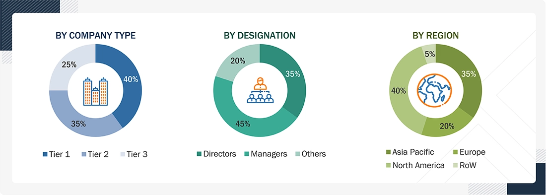
Notes: Other designations include technology heads, media analysts, sales managers, marketing managers, and product managers.
The three tiers of the companies are based on their total revenue as of 2024; Tier 1: >USD 1 billion, Tier 2: USD 500 million–1 billion, and Tier 3: USD 500 million.
To know about the assumptions considered for the study, download the pdf brochure
Market Size Estimation
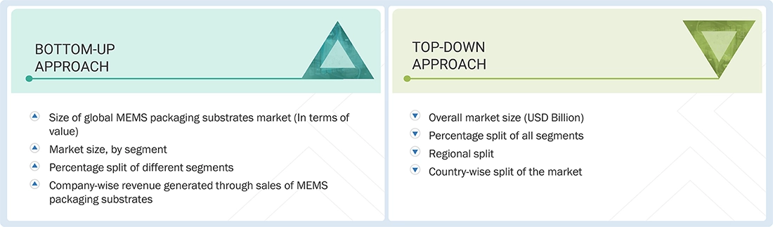
In the complete market engineering process, both top-down and bottom-up approaches are used, along with various data triangulation methods, to estimate and forecast the market size and its segments and subsegments listed in the report. Extensive qualitative and quantitative analyses have been conducted on the entire market engineering process to outline the key information and insights related to the MEMS packaging substrates market.
The key players in the market have been identified through secondary research, and their rankings in different regions have been established through both primary and secondary research. This process involved analyzing the annual and financial reports of leading companies and conducting interviews with industry experts, such as chief executive officers, vice presidents, directors, and marketing executives, to gather quantitative and qualitative insights. All percentage shares, splits, and breakdowns were determined using secondary sources and verified with primary sources. All factors influencing the markets covered in this study were carefully considered, examined in detail, validated through primary research, and analyzed to produce final quantitative and qualitative data. This data has been compiled and enriched with detailed input and analysis from MarketsandMarkets and is presented in this report.
Bottom-Up Approach
- Identifying companies dealing in MEMS packaging substrates that influence the entire market, along with related equipment players
- Analyzing major MEMS packaging substrates manufacturers, studying their portfolios, and understanding the equipment used
- Analyzing trends regarding the use of MEMS packaging substrates in different verticals, such as consumer electronics, automotive, aerospace, defense, industrial, healthcare, and telecom.
- Tracking the ongoing and upcoming developments, such as investments, R&D activities, product launches, collaborations, and partnerships in the market, along with forecasting the market based on these developments and other critical parameters
- Conducting multiple discussions with key opinion leaders to understand different equipment used for various verticals and recent trends in the market, thereby analyzing the breakdown of the scope of work carried out by major system manufacturers
- Arriving at the market estimates by analyzing the revenue generated by these companies based on their locations (countries) and combining this data to get the market estimate by region
- Verifying and cross-checking the estimates at every level via discussions with key opinion leaders, such as CXOs, directors, and operations managers, and finally with domain experts at MarketsandMarkets
- Studying various paid and unpaid sources of information, such as annual reports, press releases, white papers, and databases
Top-Down Approach
- Focusing initially on top-line investments being made in the MEMS packaging substrates ecosystem
- Calculating the market size considering the revenue generated by players through the sale of MEMS packaging substrates
- Obtaining further splits based on R&D activities and key developments in key market areas
- Deriving splits based on the use of MEMS packaging substrates in diverse verticals
- Building and developing the information related to revenue generated by players through
- their offerings
- Conducting multiple on-field discussions with key opinion leaders across major companies involved in the development of MEMS packaging substrates
- Estimating the geographic split with the help of secondary sources based on various factors, such as the number of players in a specific country/region and systems used in various verticals, such as consumer electronics, automotive, aerospace, defense, industrial, healthcare, and telecom
MEMS Packaging Substrates Market: Top-Down and Bottom-Up Approach
Data Triangulation
After arriving at the overall market size through the market size estimation process described above, the total market has been divided into several segments and subsegments. To complete the overall market engineering process and obtain precise statistics for all segments and subsegments, market breakdown and data triangulation procedures have been used wherever applicable. The data have been triangulated by examining various factors and trends from both demand and supply perspectives. Additionally, the market has been validated using top-down and bottom-up approaches.
Market Definition
A MEMS packaging substrate is the essential material layer used to support, protect, and electrically connect micro-electro-mechanical systems (MEMS) devices such as sensors and actuators. It functions as both a mechanical base and an electrical interface, ensuring signal transmission, thermal management, and environmental protection for sensitive MEMS structures. These substrates, typically made from materials like silicon, glass, ceramics, or organics, play a crucial role in enabling miniaturization, high-density integration, and reliable performance in compact electronic systems.
Key Stakeholders
- Raw material suppliers
- Substrate and wafer manufacturers
- Government bodies, venture capitalists, and private equity firms
- MEMS foundries/device manufacturers
- Packaging & assembly service providers
- Equipment and technology providers
- End-use industries
- Research institutions and industry consortia
Report Objectives
- To define, describe, segment, and forecast the size of the MEMS packaging substrate market, in terms of substrate type, application, vertical, and region
- To forecast the size of the market segments for four major regions: North America, Europe, Asia Pacific, and RoW
- To give detailed information regarding drivers, restraints, opportunities, and challenges influencing the growth of the market
- To provide value chain analysis, ecosystem analysis, case study analysis, patent analysis, trade analysis, technology analysis, pricing analysis, key conferences and events, key stakeholders and buying criteria, Porter's Five Forces analysis, investment and funding scenario, and regulations pertaining to the market
- To strategically analyze micromarkets with regard to individual growth trends, prospects, and contributions to the total market
- To analyze opportunities for stakeholders by identifying high-growth segments of the market
- To strategically profile the key players, comprehensively analyze their market position in terms of ranking and core competencies, and provide a competitive market landscape
- To analyze strategic approaches, such as product launches, acquisitions, agreements, and partnerships, in the MEMS packaging substrate market
Customization Options
With the given market data, MarketsandMarkets offers customizations according to the company’s specific needs. The following customization options are available for the report:
Company Information
- Detailed analysis and profiling of additional market players (up to 7)
Get the Full MEMS Packaging Substrates Market Report
Full forecast, segment splits, and company analysis for all MEMS Packaging Substrates Market.
- US MEMS Packaging Substrates Market
- Canada MEMS Packaging Substrates Market
- Mexico MEMS Packaging Substrates Market
- Germany MEMS Packaging Substrates Market
- France MEMS Packaging Substrates Market
- UK MEMS Packaging Substrates Market
- Italy MEMS Packaging Substrates Market
- Japan MEMS Packaging Substrates Market
- South Korea MEMS Packaging Substrates Market
- India MEMS Packaging Substrates Market
Need a Tailored Report?
Customize this report to your needs
Get 10% FREE Customization
Customize This Report