
North America Semiconductor & IC packaging materials Market (2024-2029)

The North America Semiconductor & IC packaging materials Market was valued at $7946.7 Million in 2024 and projected to reach to $12812.8 Million by 2029, representing a compound annual growth rate of 10.0%. North America's semiconductor and IC packaging materials market is poised for sustained expansion through 2029, driven by accelerating demand for advanced computing solutions and next-generation device architectures.


| Market Size in | USD 26.32 MN |
| Market Forecast in | |
| CAGR | |
| Forecast Period | |
| Units Considered | Value (USD MN) |
North America Semiconductor & IC packaging materials Market Trends and Insights
- This expansion reflects North America's critical role in global semiconductor manufacturing and advanced packaging innovation.
- The region's strong demand is driven by increasing adoption of high-performance computing, artificial intelligence, and 5G technologies that require sophisticated packaging solutions. In North America, the market growth trajectory demonstrates a compound annual growth rate of 10.0%, outpacing many mature markets globally.
- North America's leadership in semiconductor design and fabrication, combined with substantial investments in domestic chip production, continues to fuel demand for specialized packaging materials.
- Between 2024 and 2029, North America is expected to capture significant market share as manufacturers prioritize advanced packaging technologies including chiplet architectures and heterogeneous integration. North America's competitive advantage stems from its established supply chain infrastructure, technological expertise, and proximity to major semiconductor hubs.
- The region's commitment to semiconductor self-sufficiency and reshoring initiatives further strengthens demand for high-quality packaging materials throughout the forecast period..
Key Market Statistics
- CAGR (2024-2029) 10.0% CAGR
- Market Size, 2024 ~USD 7946.7 Million
- Forecast, 2029 ~USD 12812.8 Million
- Geography North America
North America Semiconductor & IC packaging materials Market Overview
Market Valuation & Growth Trajectory :
North America's semiconductor and IC packaging materials market is valued at $7,946.7 million in 2024, with a projected CAGR of 10% through 2029, reaching $12,812.8 million. This growth outpaces many global regions, positioning North America as a critical hub for advanced packaging innovation.
High-Performance Computing Demand :
The region's robust growth is primarily driven by increasing adoption of high-performance computing applications, including AI processors, data center infrastructure, and advanced consumer electronics. North American manufacturers are investing heavily in next-generation packaging technologies to meet these demands.
US Market Dominance :
The United States represents the largest market segment within North America at $9,699.3 million, accounting for the majority of regional demand. Strong semiconductor manufacturing capabilities and R&D investments in the US drive material consumption and innovation.
Strategic Regional Positioning :
North America's critical role in global semiconductor manufacturing, combined with advanced packaging innovation capabilities, positions the region as a strategic market. Canada and Mexico contribute complementary manufacturing and supply chain support, enhancing regional competitiveness.
North America Semiconductor & IC packaging materials Market Dynamics
- The region's established semiconductor ecosystem, coupled with significant capital investments in domestic manufacturing capacity, supports continued material consumption growth.
- Key drivers include the proliferation of AI and machine learning applications, 5G infrastructure deployment, and the shift toward more sophisticated packaging technologies such as chiplets and advanced interconnect solutions. The market outlook remains positive as North American manufacturers prioritize supply chain resilience and technological leadership.
- Government initiatives supporting semiconductor manufacturing, combined with private sector innovation in packaging materials, are expected to sustain the 10% CAGR through 2029.
- Strategic partnerships between material suppliers and semiconductor manufacturers will further accelerate adoption of high-performance packaging solutions across the region..
Market Ecosystem
Related Ecosystem
Resins And Polymers
- Polycarbonate
- Acrylonitrile Butadiene Styrene (ABS)
- Epoxy Resin
- Light Commercial Vehicles (LCVs)
- Polypropylene (PP)
- Basf se
- DOW CHEMICAL COMPANY
- Solvay sa
- Saudi arabia basic industries corporation (sabic)
- DuPont de Nemours, Inc.
Packaging
- Ampoules
- Gravure Process
- Rigid Packaging
- Aerosols
- Aseptic Filling and Sealing Equipment
- Amcor plc
- Essentra plc
- Berry Global Group, Inc.
- Mondi plc
- SEALED AIR CORPORATION
Speciality Chemicals
- Corrosion Inhibitors
- Polyetheretherketone (PEEK)
- Acrylonitrile Butadiene Styrene (ABS)
- Epoxy Resin
- Polycarbonate
- Basf se
- DOW CHEMICAL COMPANY
- Evonik industries ag
- Clariant ag.
- Solvay sa
Key Takeaways
- North America's semiconductor & IC packaging materials market will grow from $7,946.7M (2024) to $12,812.8M (2029) at a 10.0% CAGR
- North America's advanced manufacturing capabilities and AI/5G adoption drive sustained demand for high-performance packaging solutions
- North America's reshoring initiatives and domestic chip production investments strengthen long-term packaging materials demand
- North America commands significant competitive advantages through established supply chains and technological leadership in packaging innovation
Semiconductor & IC packaging materials Market Report Scope
| Report Metric | Details |
|---|---|
| Base Year | 2024 |
| Fastest Growing Segment | ORGANIC SUBSTRATES (Type) |
| Forecast Period | 2024-2029 |
| Growth Rate | CAGR of 10.1% from 2024 to 2029 |
| Largest Segment | CONSUMER ELECTRONICS (End-Use Industry) |
| Market Size Base Year (Billions) | ~USD 43.82 (2024) |
| Revenue Forecast (Billions) | ~USD 70.9 (2029) |
| Segments Covered | Type, Packaging Technology, End-Use Industry |
North America Semiconductor & IC packaging materials Market Report Segmentation
3 segment dimensions are covered across the global market.
By Type
- Bonding Wire
- Ceramic Packages
- Die Attach Materials
- Encapsulation Resin
- Leadframes
- Organic Substrates
- Solder Balls
- Thermal Interface Materials
By Packaging Technology
- Dfn
- Dip
- Ga
- Qfn
- Qfp
- Sop
By End-Use Industry
- Aerospace & Defense
- Automotive
- Consumer Electronics
- Healthcare
- It & Telecommunication
Target Audience
- Semiconductor Manufacturers : North American chipmakers require detailed insights into packaging material availability, pricing trends, and supplier capabilities to optimize production costs and ensure supply chain continuity for advanced packaging processes.
- Packaging Material Suppliers : Material producers need comprehensive market data on regional demand patterns, competitive positioning, and growth opportunities to expand their North American operations and capture market share in high-growth segments.
- Electronics OEMs & System Integrators : Device manufacturers depend on understanding packaging material trends to ensure component availability, manage supply chain risks, and align product development with emerging packaging technologies in North America.
- Investment & Private Equity Firms : Investors evaluating semiconductor and materials sector opportunities in North America require market sizing, growth forecasts, and competitive analysis to identify acquisition targets and assess portfolio company performance.
- Government & Policy Makers : Regulatory bodies and economic development agencies need market intelligence on North America's semiconductor packaging sector to inform industrial policy, incentive programs, and strategic manufacturing initiatives.
Countries within North America - compare and drill down
| Country | 2025 size (native) |
|---|---|
| US | USD 9699.3 Million |
| Canada | USD 1870.7 Million |
| Mexico | USD 1242.8 Million |
Country market size visualization
Reasons to Buy this Report
- Regional Market Segmentation : Gain detailed insights into North America's $7.9B market with country-level breakdowns for the US, Canada, and Mexico. Understand market dynamics specific to each North American economy and their unique growth drivers.
- Competitive Landscape Analysis : Identify leading packaging material suppliers and manufacturers operating in North America. Benchmark your position against regional competitors and understand market consolidation trends affecting the semiconductor supply chain.
- Technology & Application Trends : Explore emerging packaging technologies driving North American demand, including chiplet architectures, advanced interconnects, and thermal management solutions. Stay ahead of innovation cycles in high-performance computing and AI applications.
- Investment & Expansion Opportunities : Discover strategic opportunities for market entry, partnerships, and capacity expansion across North America. Leverage data on manufacturing investments, government incentives, and supply chain gaps to guide business decisions.
- Forecast-Driven Planning : Access 5-year projections through 2029 with 10% CAGR growth expectations. Plan production capacity, R&D investments, and market strategies based on reliable regional forecasts and demand scenarios.
Frequently asked questions
What is the current market size of semiconductor & IC packaging materials in North America?
North America's semiconductor & IC packaging materials market was valued at $7,946.7 million in 2024, representing a substantial segment of the global market.
What is the projected market size for North America by 2029?
North America's market is forecasted to reach $12,812.8 million by 2029, reflecting consistent growth throughout the forecast period.
What is the CAGR for North America's semiconductor & IC packaging materials market?
North America's market is expected to grow at a compound annual growth rate of 10.0% from 2024 to 2029.
What factors are driving growth in North America's packaging materials market?
North America's growth is driven by increased semiconductor manufacturing capacity, AI and 5G technology adoption, advanced packaging innovations, and government-backed reshoring initiatives.
How does North America's market growth compare to global trends?
North America's 10.0% CAGR aligns closely with the global market CAGR of 10.1%, demonstrating that the region maintains competitive parity with worldwide semiconductor packaging materials demand.
RESEARCH METHODOLOGY
The study involved four major activities in estimating the market size of the Semiconductor & IC packaging materials market. Exhaustive secondary research was done to collect information on the market, the peer market, and the parent market. The next step was to validate these findings, assumptions, and sizing with industry experts across the value chain through primary research. Both top-down and bottom-up approaches were employed to estimate the complete market size. Thereafter, the market breakdown and data triangulation procedures were used to estimate the market size of the segments and subsegments.
Secondary Research
In the secondary research process, various secondary sources have been referred to for identifying and collecting information for this study. These secondary sources include annual reports, press releases, investor presentations of companies, white papers, certified publications, trade directories, articles from recognized authors, the gold standard and silver standard websites, and databases.
Secondary research has been used to obtain key information about the value chain of the industry, the monetary chain of the market, the total pool of key players, market classification, and segmentation according to industry trends to the bottom-most level and regional markets. It was also used to obtain information about the key developments from a market-oriented perspective.
Primary Research
The semiconductor & IC packaging materials market comprises several stakeholders in the value chain, which include raw material suppliers, research & development, manufacturers, distribution and logistics, and end users. Various primary sources from the supply and demand sides of the semiconductor & IC packaging materials market have been interviewed to obtain qualitative and quantitative information. The primary interviewees from the demand side include key opinion leaders in end-use sectors. The primary sources from the supply side include manufacturers, associations, and institutions involved in the semiconductor & IC packaging materials industry.
Primary interviews were conducted to gather insights such as market statistics, data on revenue collected from the products and services, market breakdowns, market size estimations, market forecasting, and data triangulation. Primary research also helped in understanding the various trends related to packaging technology, type, end-use industry and region. Stakeholders from the demand side, such as CIOs, CTOs, and CSOs, were interviewed to understand the buyer’s perspective on the suppliers, products, fabricators, and their current usage of semiconductor & IC packaging materials and the outlook of their business, which will affect the overall market.
The breakdown of profiles of the primary interviewees is illustrated in the figure below:
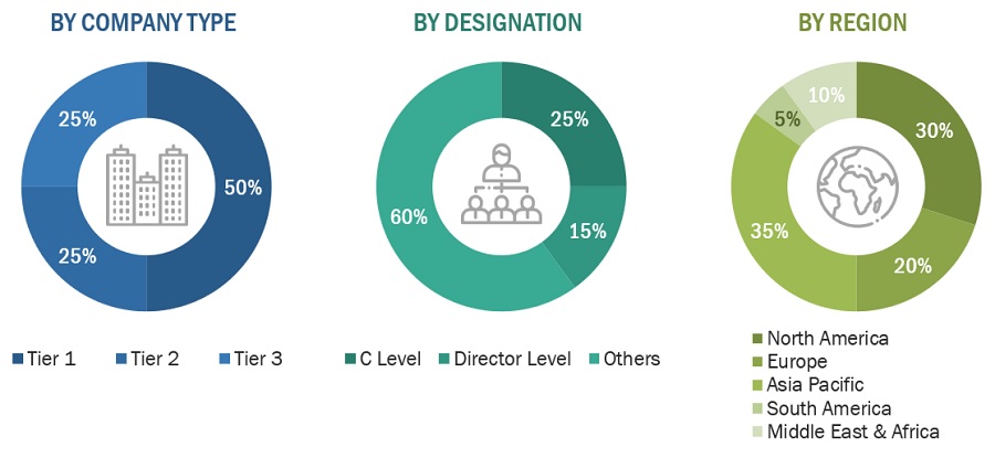
Note: Tier 1, Tier 2, and Tier 3 companies are classified based on their market revenue in 2022, available in the public domain, product portfolios, and geographical presence.
Other designations include consultants and sales, marketing, and procurement managers.
To know about the assumptions considered for the study, download the pdf brochure
|
Company name |
Designation |
|
LG Chem Ltd. (South Korea) |
Individual Industry Expert |
|
Henkel AG & Co. KGaA (Germany) |
Sales Manager |
|
Kyocera Corporation (Japan) |
Manager |
|
ASE (Taiwan) |
Marketing Manager |
|
Powertech Technology Inc. (Taiwan) |
Senior Scientist |
Market Size Estimation
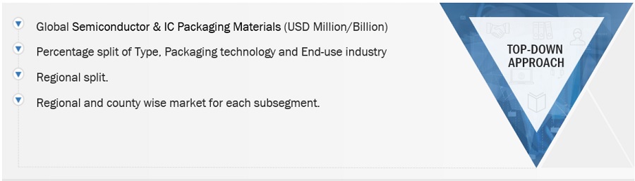
The top-down and bottom-up approaches have been used to estimate and validate the size of the Semiconductor & IC packaging materials market.
- The key players in the industry have been identified through extensive secondary research.
- The industry's supply chain has been determined through primary and secondary research.
- All percentage shares, splits, and breakdowns have been determined using secondary sources and verified through primary sources.
- All possible parameters that affect the markets covered in this research study have been accounted for, viewed in extensive detail, verified through primary research, and analyzed to obtain the final quantitative and qualitative data.
- The research includes the study of reports, reviews, and newsletters of the key market players, along with extensive interviews for opinions with leaders such as directors and marketing executives.
Semiconductor & Ic Packaging Materials Market: Bottum-Up Approach
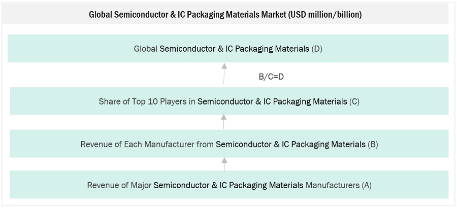
Note: All the shares are based on the global market size.
Source: Secondary Research, Interviews with Experts, and MarketsandMarkets Analysis
To know about the assumptions considered for the study, Request for Free Sample Report
Semiconductor & Ic Packaging Materials Market: Top-Down Approach
Data Triangulation
After arriving at the total market size from the estimation process explained above, the overall market has been split into several segments and sub-segments. To complete the overall market engineering process and arrive at the exact statistics for all the segments and sub-segments, the data triangulation and market breakdown procedures have been employed, wherever applicable. The data has been triangulated by studying various factors and trends from both the demand and supply sides. Along with this, the market size has been validated by using both the top-down and bottom-up approaches and primary interviews. Hence, for every data segment, there have been three sources—top-down approach, bottom-up approach, and expert interviews. The data was assumed correct when the values arrived from the three sources matched.
Market Definition
The semiconductor and IC packaging materials market refers to the industry segment focused on producing materials essential for packaging and protecting semiconductor devices and integrated circuits (ICs). These materials include organic substrates, bonding wires, leadframes, encapsulation resins, thermal insulation materials, and solder balls. The market caters to various end-use industries such as consumer electronics, automotive, aerospace, healthcare, and telecommunications. Key factors driving this market include technological advancements, demand for compact and lightweight packaging solutions, rising consumer electronics adoption, and the growth of emerging technologies like AI, IoT, and 5G.
Key Stakeholders
- Semiconductor & IC packaging materials manufacturers
- Semiconductor & IC packaging materials traders, distributors, and suppliers
- End-use industry participants of different segments of the semiconductor & IC packaging materials market
- Government and research organizations
- Associations and industrial bodies
- Research and consulting firms.
- Research & development (R&D) institutions.
Report Objectives
- To define, describe, and forecast the size of the semiconductor & IC packaging materials market, in terms of value.
- To provide detailed information regarding the major factors (drivers, opportunities, restraints, and challenges) influencing the growth of the market
- To estimate and forecast the market size based on type, packaging technology, end-use industry and region.
- To forecast the size of the market with respect to major regions, namely, Europe, North America, Asia Pacific, Middle East & Africa, and South America, along with their key countries.
- To strategically analyze micromarkets1 with respect to individual growth trends, prospects, and their contribution to the overall market.
- To analyze opportunities in the market for stakeholders and provide a competitive landscape of market leaders.
- To track and analyze recent developments such as expansions, new product launches, partnerships & agreements, and acquisitions in the market.
- To strategically profile key market players and comprehensively analyze their core competencies.
Available Customizations
Along with the given market data, MarketsandMarkets offers customizations according to the company’s specific needs. The following customization options are available for the report:
Regional Analysis
- Further breakdown of a region with respect to a particular country or additional application
Company Information
- Detailed analysis and profiles of additional market players
Get the Full Semiconductor & IC packaging materials Market Report
Full forecast, segment splits, and company analysis for all Semiconductor & IC packaging materials Market.
- China Semiconductor & IC packaging materials Market
- Japan Semiconductor & IC packaging materials Market
- India Semiconductor & IC packaging materials Market
- South Korea Semiconductor & IC packaging materials Market
- Taiwan Semiconductor & IC packaging materials Market
- Canada Semiconductor & IC packaging materials Market
- Mexico Semiconductor & IC packaging materials Market
- US Semiconductor & IC packaging materials Market
- Germany Semiconductor & IC packaging materials Market
- Italy Semiconductor & IC packaging materials Market
- France Semiconductor & IC packaging materials Market
- UK Semiconductor & IC packaging materials Market
- Spain Semiconductor & IC packaging materials Market
- UAE Semiconductor & IC packaging materials Market
- Israel Semiconductor & IC packaging materials Market
- South Africa Semiconductor & IC packaging materials Market
- Argentina Semiconductor & IC packaging materials Market
- Brazil Semiconductor & IC packaging materials Market
- Rest Of Europe Semiconductor & IC packaging materials Market
- Rest Of Asia Pacific Semiconductor & IC packaging materials Market
- Rest Of GCC Semiconductor & IC packaging materials Market
- Rest Of South America Semiconductor & IC packaging materials Market
Need a Tailored Report?
Customize this report to your needs
Get 10% FREE Customization
Customize This Report