
Hybrid Bonding Market Size, Share and Trends

Hybrid Bonding Market Size, Share & Trends By Wafer-to-Wafer (W2W), Die-to-Wafer (D2W), Die-to-Die (D2D), Wafer Bonder, Surface Prep Tool, Inspection & Metrology Tool, Cleaning & CMP System, 2.5D Packaging, and 3D Stacked IC - Global Forecast to 2032


HYBRID BONDING MARKET SIZE, SHARE & TRENDS
According to Marketsandmarkets, The global hybrid bonding market size was valued at USD 164.7 million in 2025 and is projected to reach USD 633.9 million by 2032, growing at a CAGR of 21.2%. from 2025 to 2032.. The market is driven by the semiconductor industry’s shift toward 3D integration to overcome scaling limits and achieve higher bandwidth, lower power, and finer interconnect density. Rising adoption of chiplets, advanced logic, memory stacking, and CIS devices further accelerates the demand for ultra-precise bonding processes. Expanding investments in advanced packaging by foundries and IDMs strengthen market uptake, supported by growing requirements from AI, HPC, and mobile electronics. Continuous improvements in equipment capability and process automation also enable broader high-volume manufacturing adoption.
MARKET SNAPSHOT TABLE
| REPORT METRIC | DETAILS |
|---|---|
| Market Size in 2025 (Value) | USD 164.7 Million |
| Market Forecast in 2032 (Value) | USD 633.9 Million |
| Growth Rate | CAGR of 21.2% from 2025-2032 |
| Years Considered | 2021-2032 |
| Base Year | 2024 |
| Forecast Period | 2025-2032 |
| Units Considered | Value (USD Million/Billion) and Volume (Million Units) |
| Report Coverage | Revenue forecast, company ranking, competitive landscape, growth factors, and trends |
| Top Companies |
|
| Growth Driver |
|
| Segments Covered |
|
| Regions Covered | North America, Europe, Asia Pacific, and RoW |
Market Size & Forecast
KEY TAKEAWAYS
-
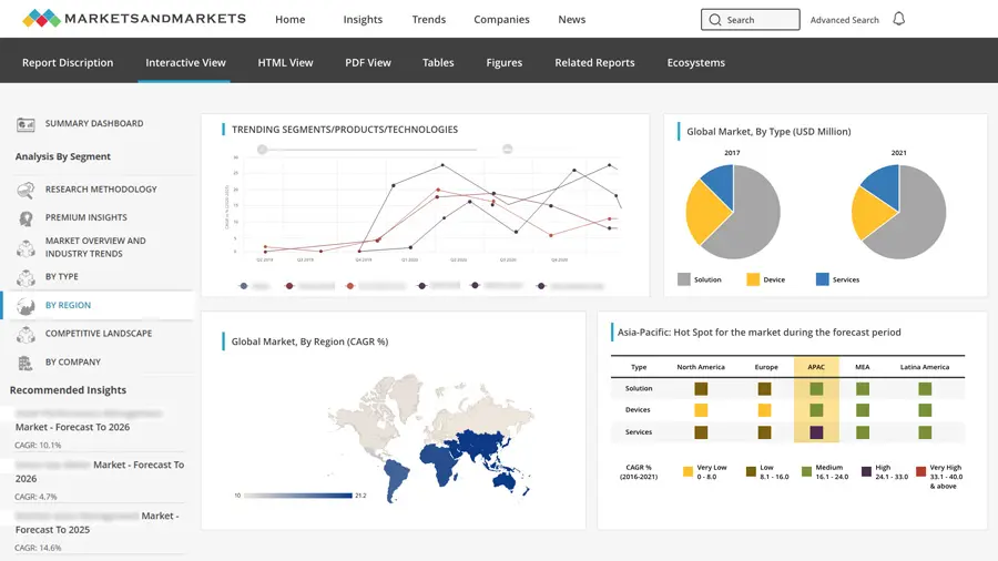
BY REGIONThe Asia Pacific hybrid bonding market accounted for a 51.6% revenue share in 2024.
-
BY PACKAGING ARCHITECTUREDie-to-die (D2D) to exhibit a CAGR of 35.3% between 2025 and 2032.
-
BY PROCESS FLOWBy process flow, the back-end segment is expected to dominate the market during the forecast period.
-
BY EQUIPMENT TYPEBy equipment type, the wafer bonders segment is likely to exhibit the highest CAGR from 2025 to 2032.
-
BY INTEGRATION LEVELBy integration level, the heterogeneous integration devices segment is projected to exhibit the fastest growth rate during the forecast peirod.
-
BY BONDING TYPEBy bonding type, copper-to-copper (Cu-Cu) is expected to lead the market and exhibit the fastest growth rate.
-
BY APPLICATIONBy application, the computing & logic segment is expected to expand with a CAGR of 26.0% from 2025 to 2032.
-
BY VERTICALBy vertical, the IT & telecommunications segment is expected to hold the largest market share in 2025.
-
Competitive LandscapeEV Group (EVG), SUSS MicroTec SE, and Applied Materials, Inc. were identified as some of the star players in the hybrid bonding market share (global), given their strong market share and product footprint.
-
Competitive LandscapeSET Corporation, Beijing U-Precision Tech, and Applied Microengineering, among others, have distinguished themselves among startups and SMEs by securing strong footholds in specialized niche areas, underscoring their potential as emerging market leaders.
Hybrid bonding adoption is rising as chipmakers transition toward 3D integration and chiplet architectures to meet performance, power, and miniaturization demands. Increasing requirements for ultra-fine-pitch interconnects in AI, HPC, memory, and advanced logic devices further accelerate its use. Foundry and IDM investments in advanced packaging lines, along with improvements in bonding accuracy, surface preparation, and metrology, are strengthening ecosystem maturity. Growing volumes of stacked CIS and next-generation mobile processors also support sustained market growth.

Source: Secondary Research, Interviews with Experts, MarketsandMarkets Analysis
TRENDS & DISRUPTIONS IMPACTING CUSTOMERS' CUSTOMERS
The hybrid bonding industry is undergoing a significant transformation, driven by the rapid shift toward high-density 3D integration across memory, logic, photonics, and heterogeneous chiplet architectures. As device scaling through traditional BEOL interconnects reaches its physical and economic limits, hybrid bonding is emerging as a disruptive enabler, offering ultra-fine pitch connectivity, lower latency, and improved power efficiency. hybrid bonding market trends transition is reshaping the competitive landscape, with the demand accelerating for advanced wafer bonders, precision alignment systems, and specialized surface-prep, cleaning, and metrology equipment. At the same time, the rise of AI accelerators, HBM, and co-packaged optics is expanding hybrid bonding into new application domains, compelling equipment vendors and semiconductor manufacturers to reorient their investment priorities toward next-generation packaging technologies.

Source: Secondary Research, Interviews with Experts, MarketsandMarkets Analysis
HYBRID BONDING MARKET DYNAMICS
Level
-
Rising demand for high-bandwidth, low-latency interconnects in AI, HPC, and logic-memory systems

-
Increasing reliance on advanced hybrid bonding to power >200-layer 3D memory

Level
-
Substantial upfront capital investment

-
Stringent environment and surface quality requirements

Level
-
Rising need for ultra-dense logic-to-memory connectivity in AI/ML accelerators

-
Deployment of hybrid bonding in CIS and AR/VR sensors to improve SNR and pixel density

Level
-
Issues in maintaining ultra-low defectivity across wafers

-
Lack of standardization in die formats, pad structures, and surface pre-treatment flows

Source: Secondary Research, Interviews with Experts, MarketsandMarkets Analysis
Driver: Rising demand for high-bandwidth, low-latency interconnects in AI, HPC, and logic-memory systems
The growth of AI workloads, HPC architectures, and advanced logic-memory systems drives the need for tighter integration and faster data transfer between chips. Traditional packaging approaches cannot support the required bandwidth and latency targets. Hybrid bonding enables ultra-fine-pitch interconnects that significantly improve performance, making it a critical enabler for next-generation compute systems.
Restraint: Substantial upfront capital investment
Hybrid bonding adoption requires expensive equipment for wafer bonding, metrology, cleaning, and alignment, creating a high entry barrier for new and smaller players. Fabs must commit significant capital to upgrade or build advanced packaging lines. This financial burden can slow down broad market penetration despite strong demand for 3D integration.
Opportunity: Rising need for ultra-dense logic-to-memory connectivity in AI/ML accelerators
AI/ML accelerators increasingly rely on tightly coupled logic and memory to support massive parallelism and rapid data movement. Hybrid bonding enables extremely dense vertical interconnects that conventional bump-based methods cannot achieve. As AI workloads scale, the requirement for such dense connectivity is intensifying, accelerating hybrid bonding adoption.
Challenge: Issues in maintaining ultra-low defectivity across wafers
Hybrid bonding requires exceptionally clean, particle-free surfaces and precise wafer alignment to achieve void-free bonds. Maintaining ultra-low defectivity across large wafers remains a technical challenge, often affecting yield and increasing process complexity. Ensuring consistent surface quality, activation, and metrology remains a major operational hurdle for high-volume manufacturing.
hybrid-bonding-market: COMMERCIAL USE CASES ACROSS INDUSTRIES
| COMPANY | USE CASE DESCRIPTION | BENEFITS |
|---|---|---|
 |
Wafer bonding, debonding, and lithography systems supporting ultra-fine-pitch hybrid bonding for W2W and D2W integration | Higher bonding precision | Improved interconnect density | Lower defect rates | Stable high-volume manufacturing performance |
 |
Lithography, wafer bonding, and plasma activation tools enabling clean surfaces and tight overlay accuracy for hybrid bonding | Better bond quality | Reduced contamination | Consistent alignment | Reliable process repeatability |
 |
Surface prep, CMP, deposition, and inspection systems integrated into hybrid bonding process flows | Superior surface cleanliness | Fewer voids | Stronger bonds | Enhanced manufacturing efficiency |
 |
High-accuracy die-bonding and placement systems optimized for D2W hybrid bonding and chiplet integration | Fine-pitch die placement | Higher throughput | Improved yields | Scalable multi-die packaging |
 |
Precision die attach and thermo-compression platforms adapted for hybrid bonding assembly | Uniform bonding results | Reduced stress | Flexible integration | Dependable production for 3D architectures |
Logos and trademarks shown above are the property of their respective owners. Their use here is for informational and illustrative purposes only.
HYBRID BONDING MARKET ECOSYSTEM
The hybrid bonding companies ecosystem is supported by a coordinated network of process developers, raw material suppliers, equipment manufacturers, and end users. Process development institutes drive innovation in bonding techniques, alignment precision, and surface preparation. Material suppliers provide specialty chemicals, CMP slurries, and bonding films essential for ultra-clean, low-defect interfaces. Equipment manufacturers enable high-volume implementation through advanced bonding, metrology, and activation tools, while major semiconductor companies adopt hybrid bonding to meet performance demands in logic, memory, CIS, and AI/HPC devices.

Logos and trademarks shown above are the property of their respective owners. Their use here is for informational and illustrative purposes only.
HYBRID BONDING MARKET SEGMENTS

Source: Secondary Research, Interviews with Experts, MarketsandMarkets Analysis
Hybrid Bonding Market, Packaging Architecture
Die-to-die hybrid bonding is growing fastest due to the rapid adoption of chiplet architectures and heterogeneous integration in AI, HPC, and advanced logic devices. D2D enables flexible design partitioning, reduced reticle limits, and highly dense interconnects between disaggregated dies. As chipmakers shift toward modular architectures to improve performance, yield, and cost efficiency, D2D bonding sees the highest acceleration in demand.
Hybrid Bonding Market, Equipment Type
Wafer bonders dominate the hybrid bonding market as wafer-to-wafer (W2W) bonding remains the primary method for achieving high throughput and uniform interconnect density in advanced packaging. Their ability to deliver precise alignment, particle-free interfaces, and stable bonding performance makes them essential for memory stacking, CIS, and high-volume manufacturing. As fabs scale 3D integration capacity, wafer bonders remain the foundational equipment category driving most capital expenditure.
Hybrid Bonding Market, Application
Computing & logic applications require extremely high bandwidth, low latency, and tight logic-to-memory coupling—needs that hybrid bonding uniquely addresses through ultra-fine-pitch interconnects. The rise of AI accelerators, HPC processors, and advanced data-center logic further amplifies the demand for 3D stacking. As architectures shift to chiplets and multi-die logic systems, this segment becomes the fastest-growing adopter of hybrid bonding.
Hybrid Bonding Market, Vertical
IT & telecommunications remain the largest segment in 2025 due to their continuous need for high-performance processors, memory technologies, and data-center infrastructure. Hybrid bonding enhances system throughput, power efficiency, and integration density—critical for cloud computing, 5G networks, and AI-driven workloads. Strong volume demand from server, networking, and communication equipment manufacturers ensures this segment retains the highest overall share.
HYBRID BONDING MARKET BY REGION
Asia Pacific to exhibit the highest CAGR in the global hybrid bonding market during the forecast period
Asia Pacific will dominate the hybrid bonding market growth due to its strong concentration of leading foundries, IDMs, and memory manufacturers that are aggressively scaling advanced packaging and 3D integration capacity. The region benefits from robust investments in semiconductor infrastructure, government support, and a mature supply chain spanning wafer fabrication, materials, and equipment. High-volume production of logic, memory, CIS, and chiplet-based devices in Taiwan, South Korea, China, and Japan further accelerates adoption. This combination of manufacturing scale, technology leadership, and continued capex expansion positions the region as the clear global leader in hybrid bonding.

hybrid-bonding-market: COMPANY EVALUATION MATRIX
The quadrant assesses companies based on their market share and product footprint within the hybrid bonding ecosystem, distinguishing established Stars with strong technological breadth from Emerging Leaders that are rapidly expanding their capabilities. EV Group stands out in the Stars quadrant due to its leadership in wafer bonding technologies, broad product portfolio, and proven adoption across high-volume logic, memory, and CIS applications. ASMPT, positioned among the Emerging Leaders, reflects growing strength in advanced packaging and die bonding solutions, supported by an expanding product footprint and increasing relevance in next-generation hybrid bonding workflows.

Source: Secondary Research, Interviews with Experts, MarketsandMarkets Analysis
KEY MARKET PLAYERS
- EV Group (EVG) (Austria)
- Applied Materials, Inc. (US)
- SUSS MicroTec SE (Germany)
- Besi (Netherlands)
- Kulicke & Soffa Industries, Inc. (Singapore)
- Tokyo Electron (TEL) (Japan)
- ASMPT (Singapore)
- Lam Research Corporation (US)
- SHIBAURA MECHATRONICS CORPORATION (Japan)
- Hanmi Semiconductor (South Korea)
- Onto Innovation (US)
- DISCO Corporation (Japan)
- TORAY ENGINEERING Co., Ltd. (Japan)
- KLA Corporation (US)
- BEIJING U-PRECISION TECH CO., LTD (China)
WHAT IS IN IT FOR YOU: hybrid-bonding-market REPORT CONTENT GUIDE

DELIVERED CUSTOMIZATIONS
We have successfully delivered the following deep-dive customizations:
| CLIENT REQUEST | CUSTOMIZATION DELIVERED | VALUE ADDS |
|---|---|---|
| Global IDM Semiconductor Manufacturer | Comprehensive benchmarking of hybrid bonding equipment, metrology tools, and surface prep systems across Tier-1 fabs | Strengthened hybrid bonding procurement strategy, improved yield optimization, and enhanced bonding process control |
| Asia Pacific Foundry | Assessment of automation readiness for hybrid bonding lines, including wafer handling, alignment systems, and activation tools | Enabled roadmap for automation scaling, improved throughput, and reduced integration variability |
| North American IDM | Evaluation of hybrid bonding materials, cleaning chemistries, and surface preparation compatibility across suppliers | Identified cost-effective materials, improved process reliability, and ensured high bonding uniformity |
| Global Tier-1 Cleanroom Equipment Supplier | Competitive benchmarking of hybrid bonding platforms, activation modules, and inspection systems | Enhanced product positioning, informed R&D priorities, and strengthened differentiation in advanced packaging |
| Asia Pacific Memory & Logic Fab | Analysis of hybrid bonding process optimization opportunities in W2W and D2W bonding for 3D stacking applications | Improved energy efficiency, enhanced ESG compliance, and increased overall bonding line productivity |
RECENT DEVELOPMENTS IN HYBRID BONDING MARKET
- September 2025 : EVG introduced the EVG 40 D2W, the industry’s first dedicated die-to-wafer overlay metrology platform designed to perform 100% die overlay measurements on 300 mm wafers with exceptional precision and production-level speed. Offering up to 15 times higher throughput than EVG’s benchmark EVG 40 NT2 hybrid wafer bonding metrology system, the EVG40 D2W enables chip manufacturers to verify die placement accuracy and implement rapid corrective measures, enhancing process control and yield in high-volume manufacturing (HVM) environments.
- September 2025 : ASMPT and KOKUSAI ELECTRIC CORPORATION entered a Joint Development Agreement (JDA) to collaboratively advance hybrid bonding (HB) and micro-bump thermo-compression bonding (TCB) technologies. This strategic partnership aims to strengthen process capabilities and deliver enhanced bonding solutions that support the growing demand for 2.5D and 3D heterogeneous integration. Through this collaboration, companies seek to accelerate the adoption of advanced packaging technologies and enable the next generation of high-performance computing (HPC) and artificial intelligence (AI) applications.
- May 2025 : SUSS MicroTec SE introduced the XBC300 Gen2 D2W platform, a customized bonding solution that completes its hybrid bonding portfolio. This new platform reinforces its leadership in delivering fully integrated die-to-wafer (D2W) hybrid bonding solutions tailored for advanced manufacturing needs. The system supports D2W bonding on 200 mm and 300 mm substrates, addressing highly stringent inter-die spacing requirements with superior precision and process control.
- April 2025 : Applied Materials acquired a 9% stake in BE Semiconductor Industries N.V. (Netherlands), a leading Dutch manufacturer of semiconductor assembly equipment, strengthening their ongoing collaboration in hybrid bonding technology for advanced chip packaging. The partnership, which began in 2020 and was recently extended, focuses on co-developing the industry’s first fully integrated die-based hybrid bonding equipment solution. This technology enables direct copper-to-copper interconnections between chiplets, a critical advancement for manufacturing high-performance, energy-efficient semiconductors that support next-generation applications such as artificial intelligence (AI).
- December 2024 : Tokyo Electron Limited introduced the Ulucus LX, an advanced Extreme Laser Lift-Off (LLO) system designed for 300 mm wafer-bonded devices. The Ulucus LX integrates laser beam irradiation, wafer separation, and wafer cleaning within a single platform, utilizing the proprietary Extreme Laser Lift-Off technology to enable efficient and precise processing for next-generation semiconductor applications.
Table of Contents
 Exclusive indicates content/data unique to MarketsandMarkets and not available with any competitors.
Methodology
The study involved major activities in estimating the current market size for the hybrid bonding market. Exhaustive secondary research was done to collect information on the market. The next step was to validate these findings, assumptions, and sizing with industry experts across the value chain using primary research. Different approaches, such as top-down and bottom-up, were employed to estimate the total market size. After that, the market breakup and data triangulation procedures were used to estimate the market size of the segments and subsegments of the hybrid bonding market.
Secondary Research
The secondary research for this study involved gathering information from credible sources. These included company annual reports, investor presentations, press releases, whitepapers, certified publications, and articles from reputable associations and government publications. Additional data was obtained from corporate filings, professional and trade associations, journals, and industry-recognized authors. Research from consortia, councils, and gold- and silver-standard websites, directories, and databases also contributed to the qualitative framework. Key global sources, such as the International Trade Centre (ITC) and the International Monetary Fund (IMF), were consulted to support and validate the market analysis.
Primary Research
Extensive primary research was conducted after understanding and analyzing the hybrid bonding market scenario through secondary research. Several primary interviews were conducted with key opinion leaders from demand- and supply-side vendors across four major regions—North America, Europe, Asia Pacific, and RoW. Approximately 20% of the primary interviews were conducted with the demand side and 80% with the supply side. Primary data was collected through questionnaires, e-mails, and telephonic interviews. Various departments within organizations, such as sales, operations, and administration, were contacted to provide a holistic viewpoint in the report.

To know about the assumptions considered for the study, download the pdf brochure
Market Size Estimation
Both top-down and bottom-up approaches were used to estimate and validate the total size of the hybrid bonding market. These methods were also used extensively to estimate the size of various subsegments in the market. The research methodology used to estimate the market size includes the following:
Hybrid Bonding Market : Top-Down and Bottom-Up Approach

Data Triangulation
After arriving at the overall size of the hybrid bonding market through the process explained above, the overall market has been split into several segments. Data triangulation procedures have been employed to complete the overall market engineering process and arrive at the exact statistics for all the segments, wherever applicable. The data has been triangulated by studying various factors and trends from the demand and supply sides. The market has also been validated using top-down and bottom-up approaches.
Market Definition
Hybrid bonding is an advanced semiconductor interconnect technology that simultaneously bonds metal-to-metal and dielectric-to-dielectric surfaces to create ultra-fine-pitch, high-density vertical connections between wafers or dies. Unlike traditional bump-based methods, hybrid bonding enables direct copper-to-copper bonding after planarization and surface activation, resulting in lower resistance, reduced parasitics, improved signal integrity, and tighter integration. It is a foundational process for 3D stacking, chiplet architectures, and next-generation logic, memory, and CIS devices.
Key Stakeholders
- Raw material suppliers
- Original equipment manufacturers (OEMs)
- Original design manufacturers (ODM)
- Research institutes
- Hybrid bonding equipment providers
- Forums, alliances, and associations
- Governments and financial institutions
- Analysts and strategic business planners
- Distributors
- End users
Report Objectives
- To describe and forecast the size of the hybrid bonding market, by packaging architecture, process flow, integration level, bonding type, equipment type, application, and vertical, in terms of value
- To describe and forecast the market size of various segments across four key regions—North America, Europe, Asia Pacific, and the Rest of the World (RoW), in terms of value
- To describe and forecast the size of the hybrid bonding market, by equipment type, in terms of volume
- To provide detailed information regarding the drivers, restraints, opportunities, and challenges influencing the growth of the hybrid bonding market
- To provide an overview of the value chain pertaining to the hybrid bonding ecosystem and the average selling prices of equipment types
- To provide a detailed overview of the impact of AI/Gen AI and the US 2025 tariff on the hybrid bonding market
- To provide information about key technological trends, trade analysis, and patents related to the hybrid bonding
- To benchmark the market players using the proprietary company evaluation matrix framework, which analyzes them on various parameters within the broad categories of market ranking/share and product portfolio
- To analyze competitive developments, such as partnerships, expansions, acquisitions, and product launches
- To strategically profile key players and analyze their market share, ranking, and core competencies
Available Customizations:
With the market data given, MarketsandMarkets offers customizations according to the company’s specific needs. The following customization options are available for the report:
Company Information
- Detailed analysis and profiling of additional market players (up to 7)
Key Questions Addressed by the Report
What is the size of the Hybrid Bonding Market?
The global Hybrid Bonding Market is estimated at USD 164.7 million in 2025 and is projected to reach USD 633.9 million by 2032, growing at a CAGR of 21.2%. from 2025 to 2032. , driven by advanced semiconductor packaging demand.
What is the expected growth rate of the Hybrid Bonding Market?
The market is expected to grow at a CAGR of 21.2% from 2025 to 2032, reflecting increasing adoption in advanced computing and semiconductor applications.
What are the key growth drivers of the Hybrid Bonding Market?
Major growth drivers include rising demand for AI and HPC processors, increasing adoption of 3D ICs, growing need for high-bandwidth and low-latency interconnects, semiconductor miniaturization, and heterogeneous integration technologies.
Why is hybrid bonding important for AI and high-performance computing applications?
Hybrid bonding enables ultra-fine-pitch interconnects, higher bandwidth, lower latency, reduced power consumption, and improved chip performance, making it critical for AI accelerators and HPC systems.
What are the major trends in the Hybrid Bonding Market?
Key trends include 3D chip stacking, chiplet architectures, advanced packaging technologies, wafer-to-wafer bonding, and increasing investment in semiconductor innovation.
Which industries are driving demand for hybrid bonding technology?
Demand is primarily driven by the semiconductor, consumer electronics, data center, artificial intelligence, automotive electronics, and telecommunications industries.
Which companies are leading the Hybrid Bonding Market?
Major players include Taiwan Semiconductor Manufacturing Company (TSMC), Samsung Electronics, SK Hynix, Intel Corporation, Applied Materials, EV Group (EVG), and Besi.
Which application segment is expected to witness significant growth?
Memory and logic device integration, AI processors, high-performance computing chips, and advanced image sensors are expected to be key growth applications for hybrid bonding technology.
Which region dominates the Hybrid Bonding Market?
Asia Pacific dominates the market due to the strong presence of semiconductor foundries, packaging facilities, and electronics manufacturers in countries such as Taiwan, South Korea, China, and Japan.
What does the Hybrid Bonding Market report analyze?
The report provides detailed analysis of market size, forecasts, technology trends, growth drivers, challenges, applications, end-use industries, competitive landscape, and regional opportunities through 2029.
Need a Tailored Report?
Customize this report to your needs
Get 10% FREE Customization
Customize This ReportPersonalize This Research
- Triangulate with your Own Data
- Get Data as per your Format and Definition
- Gain a Deeper Dive on a Specific Application, Geography, Customer or Competitor
- Any level of Personalization
Let Us Help You
- What are the Known and Unknown Adjacencies Impacting the Hybrid Bonding Market
- What will your New Revenue Sources be?
- Who will be your Top Customer; what will make them switch?
- Defend your Market Share or Win Competitors
- Get a Scorecard for Target Partners

Custom Market Research Services
We Will Customise The Research For You, In Case The Report Listed Above Does Not Meet With Your Requirements
Get 10% Free CustomisationTESTIMONIALS

Tetsuya Ohhira
Business Development Manager-Technology Business
Nikon Corporation,
Leading Japanese MNC specializing in optics and imaging productswww.nikon.com
MarketsandMarkets™ response
is quick. Their attitude is flexible and positive. Analyst Insights are globally considered and
significant. Client Services quickly respond to our inquiry and demand. Their wide range of global
surveys help us make our strategic plan.
We hope Knowledge Store will be easier to search
for a report.
VP - Marketing & Business Development
Leading Provider of Process Control Solutions
We engaged with MarketsandMarkets on a study to perform an analysis and recommend a Go-To-Market strategy for metrology and process control in the semiconductor market. The study was tailored to our targets and needs with well-defined milestones. Our overall experience with the MarketsandMarkets team was very good throughout the project in all aspects including the analysis methodologies used, the quality and depth of primary and secondary data sets, the professionalism and flexibility of the team and the ability to meet the target schedule and milestones. We want to thank MarketsandMarkets team for a job well done.
Growth opportunities and latent adjacency in Hybrid Bonding Market


Jim
Apr, 2026
How is demand from next-gen applications (AI chips, chiplets, memory stacking, high-bandwidth computing) driving adoption of hybrid bonding technologies?.
Bradley
Apr, 2026
What is the ROI outlook for investing in hybrid bonding equipment such as wafer bonders, and how do pricing trends impact profitability?.