
China Hybrid Bonding Market (2025-2030)

The China Hybrid Bonding Market was valued at $29.86 Million in 2025 and projected to reach to $134.4 Million by 2030, representing a compound annual growth rate of CAGR 24.0%. China's hybrid bonding market is poised for exceptional growth through 2030, driven by substantial government support for semiconductor self-sufficiency and aggressive R&D investments in advanced packaging technologies.


| Market Size in | USD 26.32 MN |
| Market Forecast in | |
| CAGR | |
| Forecast Period | |
| Units Considered | Value (USD MN) |
China Hybrid Bonding Market Trends and Insights
- This represents a compound annual growth rate of 24.0%, significantly outpacing global trends as China strengthens its position in advanced semiconductor packaging technologies.
- China's aggressive investment in semiconductor manufacturing and chiplet integration is driving demand for hybrid bonding solutions across high-performance computing and consumer electronics applications. The growth trajectory in China reflects the country's strategic focus on semiconductor self-sufficiency and technological advancement in interconnect solutions.
- China's hybrid bonding market is benefiting from increased adoption in data centers, artificial intelligence processors, and 5G infrastructure development.
- By 2030, China is expected to capture a substantial share of the Asia Pacific hybrid bonding market, driven by domestic chipmakers and foundries transitioning to advanced packaging architectures that require hybrid bonding capabilities..
Key Market Statistics
- CAGR (2025-2030) CAGR 24.0%
- Market Size, 2025 ~USD 29.86 Million
- Forecast, 2030 ~USD 134.4 Million
- Country China
China Hybrid Bonding Market Overview
Rapid Market Expansion :
China's hybrid bonding market is projected to grow from $29.86 million in 2025 to $134.4 million by 2030, representing a 24% CAGR that significantly exceeds the global average of 21.2%.
Government-Backed Semiconductor Push :
China's strategic investments in domestic semiconductor manufacturing and advanced packaging technologies are driving hybrid bonding adoption as a critical enabler for next-generation chiplet integration.
Chiplet Architecture Leadership :
Chinese semiconductor manufacturers are increasingly adopting hybrid bonding for chiplet-based designs, positioning the country as a key player in advanced packaging innovation and reducing reliance on foreign technologies.
Manufacturing Capacity Growth :
Expansion of Chinese foundries and packaging facilities with hybrid bonding capabilities is accelerating market penetration across consumer electronics, data centers, and automotive applications.
China Hybrid Bonding Market Dynamics
- The country's leading position in electronics manufacturing and growing chiplet adoption across multiple industries create a favorable ecosystem for hybrid bonding expansion.
- Chinese semiconductor companies are rapidly scaling production capabilities to meet domestic and international demand, while strategic partnerships with equipment suppliers strengthen the supply chain.
- This momentum positions China as a critical hub for hybrid bonding innovation and manufacturing, with opportunities extending across consumer, industrial, and automotive sectors..
Market Ecosystem
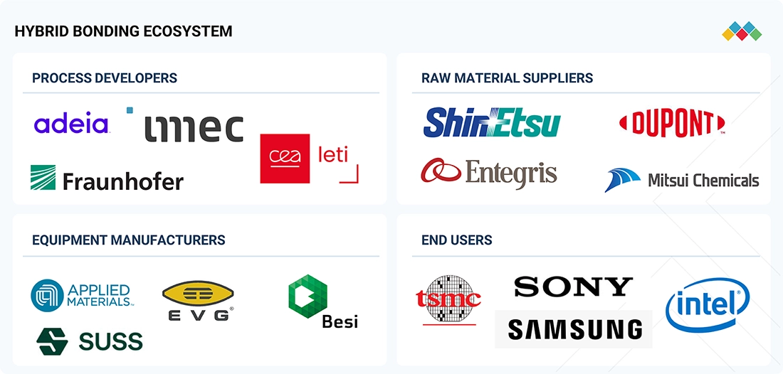
hybrid-bonding-market: COMMERCIAL USE CASES ACROSS INDUSTRIES
| COMPANY | USE CASE DESCRIPTION | BENEFITS |
|---|---|---|
 |
Wafer bonding, debonding, and lithography systems supporting ultra-fine-pitch hybrid bonding for W2W and D2W integration | Higher bonding precision | Improved interconnect density | Lower defect rates | Stable high-volume manufacturing performance |
 |
Lithography, wafer bonding, and plasma activation tools enabling clean surfaces and tight overlay accuracy for hybrid bonding | Better bond quality | Reduced contamination | Consistent alignment | Reliable process repeatability |
 |
Surface prep, CMP, deposition, and inspection systems integrated into hybrid bonding process flows | Superior surface cleanliness | Fewer voids | Stronger bonds | Enhanced manufacturing efficiency |
 |
High-accuracy die-bonding and placement systems optimized for D2W hybrid bonding and chiplet integration | Fine-pitch die placement | Higher throughput | Improved yields | Scalable multi-die packaging |
 |
Precision die attach and thermo-compression platforms adapted for hybrid bonding assembly | Uniform bonding results | Reduced stress | Flexible integration | Dependable production for 3D architectures |
Logos and trademarks shown above are the property of their respective owners. Their use here is for informational and illustrative purposes only.
Related Ecosystem
Semiconductor Materials And Components
- Sensors
- Gallium Nitride (GaN)
- Digital Signal Processor (DSP)
- Natural Language Processing (NLP)
- Silicon Carbide
- Texas Instruments Incorporated
- Samsung
- APPLIED MATERIALS, INC.
- Stmicroelectronics
- Lenovo
Key Takeaways
- China's hybrid bonding market will grow from $29.86M (2025) to $134.4M (2030) at a 24.0% CAGR, outpacing global growth rates.
- China's semiconductor self-sufficiency initiatives are accelerating hybrid bonding adoption in advanced packaging and chiplet integration.
- China's market expansion is driven by AI, data center, and 5G infrastructure investments requiring advanced interconnect technologies.
- China is positioned to become a dominant regional player in hybrid bonding by 2030, supported by domestic foundry capabilities.
Hybrid Bonding Market Report Scope
| Report Metric | Details |
|---|---|
| Base Year | 2025 |
| Fastest Growing Segment | DIE-TO-DIE (D2D) (Packaging Architecture) |
| Forecast Period | 2025–2030 |
| Growth Rate | CAGR of 21.2% from 2025 to 2030 |
| Largest Segment | BACK-END (Process Flow) |
| Market Size Base Year (Billions) | ~USD 0.17 (2025) |
| Revenue Forecast (Billions) | ~USD 0.43 (2030) |
| Segments Covered | Bonding Type, Packaging Architecture, Integration Level, Process Flow, Equipment Type, Application, Type, Vertical |
China Hybrid Bonding Market Report Segmentation
8 segment dimensions are covered across the global market.
By Bonding Type
- Copper-To-Copper (Cu-Cu)
- Copper-To-Pad /Metal-To-Pad
- Other Bonding Types
By Packaging Architecture
- Die-To-Die (D2D)
- Die-To-Wafer (D2W)
- Wafer-To-Wafer (W2W)
By Integration Level
- 2.5D Packaging
- 3D Stacked Ics
- Heterogeneous Integration
By Process Flow
- Back-End
- Front-End
By Equipment Type
- Cleaning & Cmp Systems
- Inspection & Metrology Tools
- Surface Prep Tools
- Wafer Bonders
By Application
- Computing & Logic
- Connectivity & Communications
- Memory & Storage
- Other Applications
- Sensing & Interface
By Type
- 3D Nand & Stacked Dram
- 5G Devices
- Cmos Image Sensors (Cis)
- Heterogeneous Socs & Chiplet Integration
- High-Bandwidth Memory (Hbm)
- High-Performance Computing & AI Accelerators
- MEMS & Other Sensors
- Micro-Led Displays
- Photonics & Optical Interconnects
- Rf Front-End Modules (Fem)
By Vertical
- Aerospace & Defense
- Automotive
- Consumer Electronics
- Healthcare & Medical
- Industrial Automation
- It & Telecommunications
- Other Verticals
Target Audience
- Chinese Semiconductor Manufacturers : Understand market dynamics, competitive positioning, and technology adoption trends to optimize hybrid bonding integration into product roadmaps and manufacturing strategies.
- Equipment & Materials Suppliers : Identify growth opportunities, customer segments, and demand drivers specific to China's hybrid bonding market to guide sales and product development strategies.
- Foundries & Packaging Service Providers : Assess market potential, capacity planning requirements, and service differentiation opportunities as Chinese foundries scale hybrid bonding capabilities.
- Investment & Private Equity Firms : Evaluate investment opportunities in Chinese hybrid bonding companies, equipment makers, and semiconductor manufacturers with exposure to this high-growth market segment.
- International Technology Companies : Develop market entry strategies, partnership models, and competitive positioning for the Chinese hybrid bonding market amid government support and rapid localization trends.
Key Companies in the China Hybrid Bonding Market
| Company | HQ | Ownership | Strongest segments |
|---|---|---|---|
| APPLIED MATERIALS, INC. | United States | Public Company | Wafer Bonder,Surface Prep Tool,Inspection & Metrology Tool, |
| SUSS MICROTEC SE | Germany | Public Company | Wafer Bonder (including hybrid-capable W2W/D2W tools),Surface Prep Tool,Inspection & Metrology Tool, |
| BESI | Netherlands | Public Company | Wafer Bonder (Hybrid-Capable),Die-to-Wafer (D2W) Hybrid Die Bonders,Die-to-Die (D2D) and Advanced Die Attach, |
| EV GROUP (EVG) | Canada | ||
| KULICKE AND SOFFA INDUSTRIES, INC. | Singapore | Public Company | Die-to-Wafer (D2W) Hybrid Bonding Tools,Die-to-Die (D2D) Hybrid Bonding Tools,Wafer-to-Wafer (W2W) Hybrid Bonders, |
| TOKYO ELECTRON LIMITED | Japan | Public Company | Wafer-to-Wafer (W2W),Die-to-Wafer (D2W),Die-to-Die (D2D), |
| LAM RESEARCH CORPORATION | United States | Public Company | Surface Prep Tool,Cleaning & CMP System,Surface-Related Etch (Dielectric/TSV), |
| SHIBAURA MECHATRONICS CORPORATION | Japan | Public Company | Cleaning & CMP System,Surface Prep Tool,Wafer Bonder, |
| ASMPT | Singapore | Public Company | Die-to-Wafer (D2W) Hybrid Bonders,Die-to-Die (D2D) Hybrid Bonders,Wafer-to-Wafer (W2W) Hybrid Bonders, |
| HANMI SEMICONDUCTOR | South Korea | Public Company | Wafer Bonder (Hybrid-capable W2W and D2W),Die-to-Die and Die-to-Wafer Placement / Pick-and-Place,Inspection & Metrology Tools, |
| ONTO INNOVATION | United States | Public Company | Inspection & Metrology Tool,Surface Prep Tool,Cleaning & CMP System (Metrology/Control), |
| DISCO CORPORATION | United States | Private Company | Surface Prep Tool,Cleaning & CMP System,Inspection & Metrology Tool, |
| KLA CORPORATION | United States | Public Company | Inspection & Metrology Tool,Surface Prep Tool,Cleaning & CMP System, |
| BEIJING U-PRECISION TECH CO., LTD | China | Private Company | Precision motion stages for wafer bonder and D2W/D2D handling,Electrostatic chucks for wafer handling and bonding,Ultra-precision measurement, inspection, and metrology subsystems, |
APPLIED MATERIALS, INC.
Applied Materials, Inc. is a United States-based public company founded in 1967 with 36,500 employees. The company is a leading provider of manufacturing equipment and services for the semiconductor and display industries.
SUSS MICROTEC SE
SUSS MicroTec SE is a German public company established in 1949 with 1,484 employees. The company specializes in manufacturing equipment for microstructuring and nanotechnology applications.
BESI
BESI is a Netherlands-based public company founded in 1995 with 1,856 employees. The company provides assembly equipment and solutions for the semiconductor and electronics packaging industries.
EV GROUP (EVG)
EV Group (EVG) is a company based in Canada. Specific operational details are not provided.
KULICKE AND SOFFA INDUSTRIES, INC.
Kulicke and Soffa Industries, Inc. is a Singapore-based public company founded in 1951 with 2,551 employees. The company manufactures semiconductor assembly and packaging equipment.
TOKYO ELECTRON LIMITED
Tokyo Electron Limited is a Japanese public company established in 1951 with 20,236 employees. The company is a major provider of semiconductor production equipment and services.
LAM RESEARCH CORPORATION
Lam Research Corporation is a United States-based public company founded in 1980 with 20,600 employees. The company designs and manufactures semiconductor processing equipment for the global chip manufacturing industry.
SHIBAURA MECHATRONICS CORPORATION
Shibaura Mechatronics Corporation is a Japanese public company founded in 1939 with 1,269 employees. The company manufactures precision machinery and equipment for various industrial applications.
ASMPT
ASMPT is a Singapore-based public company established in 1975 with 9,000 employees. The company provides assembly and packaging solutions for the semiconductor and electronics industries.
HANMI SEMICONDUCTOR
Hanmi Semiconductor is a South Korea-based private company founded in 1980 with 698 employees. The company operates in the semiconductor industry.
ONTO INNOVATION
Onto Innovation is a United States-based public company founded in 1940 with 1,615 employees. The company provides process technology solutions for the semiconductor and advanced packaging industries.
DISCO CORPORATION
Disco Corporation is a United States-based private company founded in 1960 with 21,000 employees. The company manufactures precision cutting, grinding, and polishing equipment for semiconductor and electronics applications.
KLA CORPORATION
KLA Corporation is a United States-based public company founded in 2012 with 2,333 employees. The company provides process control and yield management solutions for the semiconductor industry.
BEIJING U-PRECISION TECH CO., LTD
Beijing U-Precision Tech Co., Ltd. is a China-based private company founded in 2012. Specific employee and operational details are unavailable.
Reasons to Buy this Report
- Market-Specific Growth Projections : Access detailed forecasts for China's hybrid bonding market with 24% CAGR through 2030, enabling accurate business planning and investment decisions tailored to this high-growth region.
- Competitive Landscape Intelligence : Identify key Chinese manufacturers, foundries, and packaging providers entering the hybrid bonding space, along with their strategic positioning and market share dynamics.
- Government Policy & Incentive Analysis : Understand China's semiconductor self-sufficiency initiatives, subsidies, and regulatory frameworks driving hybrid bonding adoption and manufacturing capacity expansion.
- Chiplet Adoption Trends : Gain insights into how Chinese semiconductor companies are leveraging hybrid bonding for chiplet architectures across consumer electronics, data centers, and automotive applications.
- Supply Chain & Partnership Opportunities : Discover equipment suppliers, material vendors, and strategic partnership opportunities within China's rapidly expanding hybrid bonding ecosystem.
Frequently asked questions
What is the current size of China's hybrid bonding market?
China's hybrid bonding market is valued at $29.86 million in 2025 and is projected to reach $134.4 million by 2030.
What is the growth rate of China's hybrid bonding market?
China's hybrid bonding market is growing at a compound annual growth rate (CAGR) of 24.0% from 2025 to 2030.
What are the primary drivers of growth in China's hybrid bonding market?
China's hybrid bonding market growth is driven by semiconductor self-sufficiency initiatives, AI processor development, data center expansion, and 5G infrastructure investments requiring advanced packaging technologies.
Which industries in China are adopting hybrid bonding technology?
China's hybrid bonding adoption is concentrated in high-performance computing, artificial intelligence, data centers, consumer electronics, and 5G telecommunications infrastructure.
How does China's hybrid bonding market compare to global trends?
China's hybrid bonding market CAGR of 24.0% exceeds the global CAGR of 21.2%, reflecting China's accelerated investment in advanced semiconductor packaging and domestic chipmaking capabilities.
RESEARCH METHODOLOGY
The study involved major activities in estimating the current market size for the hybrid bonding market. Exhaustive secondary research was done to collect information on the market. The next step was to validate these findings, assumptions, and sizing with industry experts across the value chain using primary research. Different approaches, such as top-down and bottom-up, were employed to estimate the total market size. After that, the market breakup and data triangulation procedures were used to estimate the market size of the segments and subsegments of the hybrid bonding market.
Secondary Research
The secondary research for this study involved gathering information from credible sources. These included company annual reports, investor presentations, press releases, whitepapers, certified publications, and articles from reputable associations and government publications. Additional data was obtained from corporate filings, professional and trade associations, journals, and industry-recognized authors. Research from consortia, councils, and gold- and silver-standard websites, directories, and databases also contributed to the qualitative framework. Key global sources, such as the International Trade Centre (ITC) and the International Monetary Fund (IMF), were consulted to support and validate the market analysis.
Primary Research
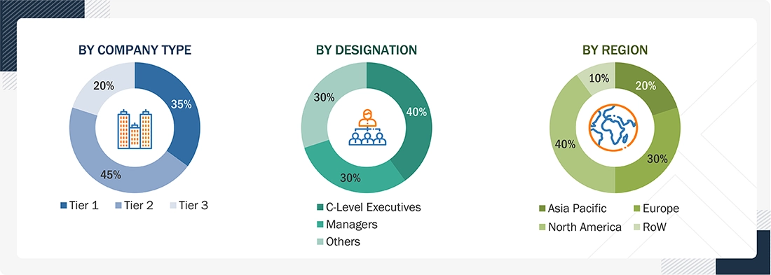
Extensive primary research was conducted after understanding and analyzing the hybrid bonding market scenario through secondary research. Several primary interviews were conducted with key opinion leaders from demand- and supply-side vendors across four major regions—North America, Europe, Asia Pacific, and RoW. Approximately 20% of the primary interviews were conducted with the demand side and 80% with the supply side. Primary data was collected through questionnaires, e-mails, and telephonic interviews. Various departments within organizations, such as sales, operations, and administration, were contacted to provide a holistic viewpoint in the report.
To know about the assumptions considered for the study, download the pdf brochure
Market Size Estimation
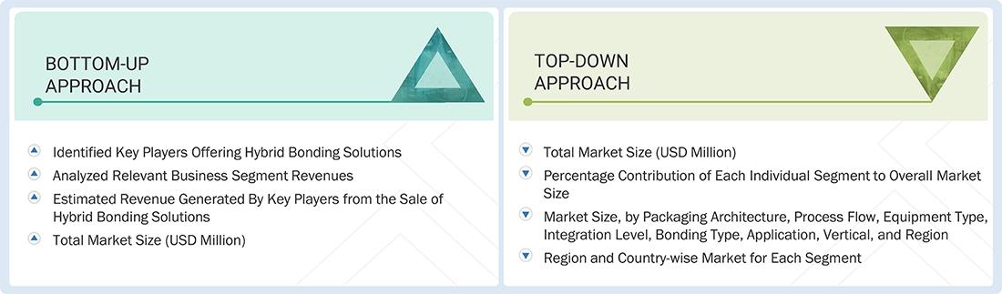
Both top-down and bottom-up approaches were used to estimate and validate the total size of the hybrid bonding market. These methods were also used extensively to estimate the size of various subsegments in the market. The research methodology used to estimate the market size includes the following:
Hybrid Bonding Market : Top-Down and Bottom-Up Approach
Data Triangulation
After arriving at the overall size of the hybrid bonding market through the process explained above, the overall market has been split into several segments. Data triangulation procedures have been employed to complete the overall market engineering process and arrive at the exact statistics for all the segments, wherever applicable. The data has been triangulated by studying various factors and trends from the demand and supply sides. The market has also been validated using top-down and bottom-up approaches.
Market Definition
Hybrid bonding is an advanced semiconductor interconnect technology that simultaneously bonds metal-to-metal and dielectric-to-dielectric surfaces to create ultra-fine-pitch, high-density vertical connections between wafers or dies. Unlike traditional bump-based methods, hybrid bonding enables direct copper-to-copper bonding after planarization and surface activation, resulting in lower resistance, reduced parasitics, improved signal integrity, and tighter integration. It is a foundational process for 3D stacking, chiplet architectures, and next-generation logic, memory, and CIS devices.
Key Stakeholders
- Raw material suppliers
- Original equipment manufacturers (OEMs)
- Original design manufacturers (ODM)
- Research institutes
- Hybrid bonding equipment providers
- Forums, alliances, and associations
- Governments and financial institutions
- Analysts and strategic business planners
- Distributors
- End users
Report Objectives
- To describe and forecast the size of the hybrid bonding market, by packaging architecture, process flow, integration level, bonding type, equipment type, application, and vertical, in terms of value
- To describe and forecast the market size of various segments across four key regions—North America, Europe, Asia Pacific, and the Rest of the World (RoW), in terms of value
- To describe and forecast the size of the hybrid bonding market, by equipment type, in terms of volume
- To provide detailed information regarding the drivers, restraints, opportunities, and challenges influencing the growth of the hybrid bonding market
- To provide an overview of the value chain pertaining to the hybrid bonding ecosystem and the average selling prices of equipment types
- To provide a detailed overview of the impact of AI/Gen AI and the US 2025 tariff on the hybrid bonding market
- To provide information about key technological trends, trade analysis, and patents related to the hybrid bonding
- To benchmark the market players using the proprietary company evaluation matrix framework, which analyzes them on various parameters within the broad categories of market ranking/share and product portfolio
- To analyze competitive developments, such as partnerships, expansions, acquisitions, and product launches
- To strategically profile key players and analyze their market share, ranking, and core competencies
Available Customizations:
With the market data given, MarketsandMarkets offers customizations according to the company’s specific needs. The following customization options are available for the report:
Company Information
- Detailed analysis and profiling of additional market players (up to 7)
Get the Full Hybrid Bonding Market Report
Full forecast, segment splits, and company analysis for all Hybrid Bonding Market.
- US Hybrid Bonding Market
- Canada Hybrid Bonding Market
- Mexico Hybrid Bonding Market
- Germany Hybrid Bonding Market
- UK Hybrid Bonding Market
- France Hybrid Bonding Market
- Italy Hybrid Bonding Market
- Spain Hybrid Bonding Market
- Nordics Hybrid Bonding Market
- Poland Hybrid Bonding Market
- Rest Of Europe Hybrid Bonding Market
- Japan Hybrid Bonding Market
- South Korea Hybrid Bonding Market
- Taiwan Hybrid Bonding Market
- India Hybrid Bonding Market
- Rest Of Asia Pacific Hybrid Bonding Market
Need a Tailored Report?
Customize this report to your needs
Get 10% FREE Customization
Customize This Report