
India Atomic Force Microscopy Market (2025-2030)

The India Atomic Force Microscopy Market was valued at $14.5 Million in 2025 and projected to reach to $23.1 Million by 2030, representing a compound annual growth rate of 9.8%. India's Atomic Force Microscopy market is poised for accelerated growth driven by the country's strategic focus on semiconductor self-sufficiency and nanotechnology innovation.


| Market Size in | USD 26.32 MN |
| Market Forecast in | |
| CAGR | |
| Forecast Period | |
| Units Considered | Value (USD MN) |
India Atomic Force Microscopy Market Trends and Insights
- This accelerated growth in India significantly outpaces the global average of 7.1%, driven by the country's expanding semiconductor manufacturing ecosystem and increasing investment in nanotechnology research.
- India's AFM market benefits from rising demand for precision measurement tools in electronics fabrication, materials science, and academic research institutions across the nation. The forecast period through 2030 reflects India's strategic positioning as a semiconductor hub and the government's push toward indigenous electronics manufacturing.
- India's adoption of AFM technology is accelerating as domestic semiconductor fabs and research organizations prioritize advanced characterization capabilities.
- The 59.3% growth projected for India between 2025 and 2030 underscores the country's commitment to building world-class manufacturing and R&D infrastructure in the semiconductor and electronics sectors..
Key Market Statistics
- CAGR (2025-2030) 9.8% CAGR
- Market Size, 2025 ~USD 14.5 Million
- Forecast, 2030 ~USD 23.1 Million
- Country India
India Atomic Force Microscopy Market Overview
Fastest Growing Market Globally :
India's AFM market CAGR of 9.8% significantly exceeds the global average of 7.1%, positioning the country as one of the most dynamic markets for atomic force microscopy technology adoption.
Semiconductor Manufacturing Boom :
India's expanding semiconductor manufacturing ecosystem, supported by government initiatives like the Production Linked Incentive (PLI) scheme, is driving substantial demand for advanced characterization tools including AFM systems.
Nanotechnology Investment Surge :
Increased government and private sector investment in nanotechnology research and development across Indian institutions is accelerating the adoption of AFM for nanoscale material analysis and quality control.
Projected Market Expansion :
The Indian AFM market is expected to grow from USD 14.5 million in 2025 to USD 23.1 million by 2030, representing a 59.3% increase in market value over the five-year forecast period.
India Atomic Force Microscopy Market Dynamics
- The government's PLI scheme and establishment of semiconductor fabrication plants are creating substantial demand for advanced analytical instruments.
- Research institutions and emerging semiconductor manufacturers are increasingly investing in AFM technology for material characterization, quality assurance, and product development. The market's 9.8% CAGR reflects India's transition toward high-tech manufacturing and R&D capabilities.
- With growing collaborations between academic institutions and industry players, coupled with rising awareness of nanotechnology applications across pharmaceuticals, electronics, and materials science, India's AFM market is expected to attract both domestic and international equipment manufacturers, further accelerating market penetration and innovation..
Market Ecosystem
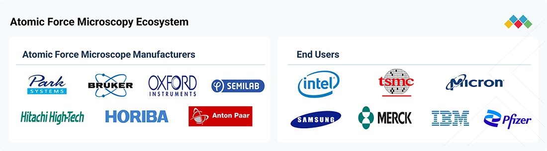
ATOMIC FORCE MICROSCOPY MARKET: COMMERCIAL USE CASES ACROSS INDUSTRIES
| COMPANY | USE CASE DESCRIPTION | BENEFITS |
|---|---|---|
 |
Park Systems provides atomic force microscope systems for semiconductor and electronics, materials science and nanotechnology, chemical and polymer research, and life sciences. Its systems are used to measure surface roughness, observe nanoscale structures, identify defects, and characterize material surfaces. | Enables detailed surface and nanoscale analysis | Supports semiconductor wafer and device characterization | Helps measure surface roughness and defects | Supports research and quality-control activities |
 |
Bruker provides atomic force microscope systems for semiconductor and electronics, materials science and nanotechnology, chemical and polymer research, and life sciences. Its systems are used to study surface topography, material properties, thin films, and biological samples at the nanoscale. | Enables high-resolution surface characterization | Supports analysis of material and mechanical properties | Helps characterize thin films and advanced materials | Supports research in materials and life sciences |
 |
Oxford Instruments provides atomic force microscope systems for materials science and nanotechnology, semiconductor and electronics, and life sciences. Its systems are used to examine surface structure, roughness, electrical properties, and other nanoscale characteristics of materials and devices. | Enables precise nanoscale surface measurements | Supports semiconductor and advanced-material research | Helps analyze electrical and surface properties | Supports detailed characterization of materials and devices |
 |
Hitachi High-Tech Corporation provides atomic force microscope systems for semiconductor and electronics, materials science and nanotechnology, and industrial applications. Its systems are used to examine wafer and material surfaces, measure roughness, and identify small surface defects and variations. | Supports wafer and surface inspection | Helps identify nanoscale defects and surface variations | Enables accurate roughness measurements | Supports semiconductor process development and quality control |
 |
Semilab provides atomic force microscope and surface-analysis solutions for semiconductor and electronics, materials science and nanotechnology, and industrial applications. Its solutions are used to analyze wafer surfaces, thin films, surface roughness, and nanoscale defects during research and manufacturing processes. | Enables detailed wafer and thin-film characterization | Supports semiconductor process monitoring | Helps identify surface defects and roughness variations | Supports research and manufacturing quality control |
Logos and trademarks shown above are the property of their respective owners. Their use here is for informational and illustrative purposes only.
Related Ecosystem
Electronics System And Components
- Sensors
- Temperature Sensors
- Pressure Sensors
- Actuators
- Image Sensors
- Lenovo
- Samsung
- Texas Instruments Incorporated
- HONEYWELL INTERNATIONAL INC.
- Teledyne Technologies Incorporated
Key Takeaways
- India's AFM market is valued at USD 14.5 million in 2025 and expected to grow to USD 23.1 million by 2030 at a 9.8% CAGR, outpacing global growth.
- India's semiconductor manufacturing expansion and government initiatives are primary drivers accelerating AFM adoption across the country.
- India's research institutions and domestic semiconductor fabs are increasingly investing in advanced characterization and nanotechnology capabilities.
- India's projected 59.3% market growth through 2030 reflects the nation's strategic focus on building indigenous electronics manufacturing infrastructure.
Atomic Force Microscopy Market Report Scope
| Report Metric | Details |
|---|---|
| Base Year | 2025 |
| Fastest Growing Segment | SOFTWARE (Offering) |
| Forecast Period | 2025-2030 |
| Growth Rate | CAGR of 7.1% from 2025 to 2030 |
| Largest Segment | ATOMIC FORCE MICROSCOPES (Offering) |
| Market Size Base Year (Billions) | ~USD 0.54 (2025) |
| Revenue Forecast (Billions) | ~USD 0.76 (2030) |
| Segments Covered | Offering, Grade, Application |
India Atomic Force Microscopy Market Report Segmentation
3 segment dimensions are covered across the global market.
By Offering
- Atomic Force Microscopes
- Probes
- Software
By Grade
- Industrial
- Research
By Application
- Chemical & Polymer Research
- Life Sciences & Biomedical
- Material Science & Nanotechnology
- Other Applications
- Semiconductors & Electronics
INDIA: ATOMIC FORCE MICROSCOPY MARKET, BY APPLICATION, 2025–2030
| Segment | 2025 | 2026 | 2027 | 2028 | 2029 | 2030 | CAGR (%) |
|---|---|---|---|---|---|---|---|
| CHEMICAL & POLYMER RESEARCH | 2.96 | 3.18 | 3.43 | 3.7 | 3.98 | 4.27 | 7.6 |
| LIFE SCIENCES & BIOMEDICAL | 2.92 | 3.27 | 3.67 | 4.13 | 4.63 | 5.17 | 12.1 |
| MATERIAL SCIENCE & NANOTECHNOLOGY | 4.11 | 4.46 | 4.87 | 5.31 | 5.78 | 6.29 | 8.9 |
| OTHER APPLICATIONS | 0.92 | 0.97 | 1.03 | 1.09 | 1.16 | 1.22 | 5.9 |
| SEMICONDUCTORS & ELECTRONICS | 3.57 | 3.97 | 4.43 | 4.94 | 5.51 | 6.11 | 11.4 |
| TOTAL | 14.47 | 15.84 | 17.43 | 19.17 | 21.05 | 23.06 | 9.8 |
Target Audience
- AFM Equipment Manufacturers : Global and regional AFM manufacturers need India-specific market data to assess market size, growth potential, and competitive positioning for product launches, distribution partnerships, and manufacturing facility decisions.
- Semiconductor & Electronics Companies : Indian and multinational semiconductor firms require detailed market insights to evaluate AFM adoption rates, supplier options, and technology trends to optimize their quality control and R&D operations.
- Research & Academic Institutions : Universities and research centers in India need market intelligence to justify AFM equipment investments, understand funding opportunities, and align nanotechnology research initiatives with industry demands.
- Investment & Private Equity Firms : Investors evaluating opportunities in India's semiconductor, nanotechnology, and advanced materials sectors require market data to assess growth potential, identify acquisition targets, and evaluate portfolio companies.
- Government & Policy Bodies : Indian government agencies and policy makers need market insights to design effective incentive schemes, allocate R&D funding, and develop strategies supporting the country's semiconductor and nanotechnology ambitions.
Reasons to Buy this Report
- India-Specific Market Sizing : Access precise valuation data for India's AFM market with verified figures for 2025 (USD 14.5M) and 2030 (USD 23.1M), enabling accurate financial forecasting and investment planning specific to the Indian market.
- Competitive Advantage Intelligence : Understand India's 9.8% CAGR advantage over global 7.1% growth, identifying unique market drivers and opportunities that competitors may overlook when entering or expanding in the Indian AFM sector.
- Semiconductor Ecosystem Insights : Gain detailed understanding of how India's expanding semiconductor manufacturing base, PLI schemes, and fab establishments are creating specific demand patterns for AFM technology and characterization services.
- Investment & Expansion Strategy : Leverage India-focused market data to develop targeted go-to-market strategies, identify key customer segments, and prioritize resource allocation for market entry or expansion in this high-growth region.
- Stakeholder Decision Support : Provide board-level executives, investors, and business development teams with credible, India-specific market intelligence to support funding decisions, partnership evaluations, and strategic planning initiatives.
Frequently asked questions
What is the current size of India's Atomic Force Microscopy market?
India's AFM market was valued at USD 14.5 million in 2025 and is projected to reach USD 23.1 million by 2030.
What is the growth rate of India's AFM market?
India's AFM market is growing at a compound annual growth rate (CAGR) of 9.8% from 2025 to 2030, significantly higher than the global average of 7.1%.
What factors are driving growth in India's AFM market?
India's AFM market growth is driven by expanding semiconductor manufacturing, government initiatives for indigenous electronics production, increased nanotechnology research, and rising demand for precision measurement tools in fabrication facilities.
Which sectors in India are adopting AFM technology?
India's semiconductor fabs, research institutions, materials science laboratories, and academic centers are the primary adopters of AFM technology for advanced characterization and quality control applications.
How does India's AFM market growth compare to global trends?
India's 9.8% CAGR significantly outpaces the global AFM market CAGR of 7.1%, reflecting India's accelerated investment in semiconductor infrastructure and nanotechnology research capabilities.
RESEARCH METHODOLOGY
The study involved four major activities in estimating the current size of the atomic force microscopy market. Extensive secondary research was conducted to gather information on the market, adjacent industries, and the broader microscopy, nanotechnology, metrology, semiconductor, materials research, and life sciences ecosystem. This was followed by primary research with industry stakeholders across the value chain, including atomic force microscope manufacturers, probe suppliers, microscopy and metrology technology providers, distributors, research institutions, system integrators, and end users across semiconductor and electronics, materials science and nanotechnology, chemical and polymer research, life sciences, and industrial applications, to validate assumptions and market sizing. Both top-down and bottom-up approaches were used to estimate the overall market size. Market breakdowns and data triangulation techniques were then applied to derive the size of individual segments and subsegments. Secondary and primary sources were jointly used to support a comprehensive technical and commercial analysis of the market.
Secondary Research
Various secondary sources were referred to during the secondary research process to identify and collect information relevant to the atomic force microscopy market. These sources included annual reports, press releases, investor presentations of key companies, product catalogs, technical datasheets, white papers, industry journals, certified publications, patents, industry associations, company websites, trade directories, government databases, and microscopy, nanotechnology, and semiconductor industry sources. Secondary research was conducted to obtain key insights into the market’s supply chain, value chain, competitive landscape, and segmentation across offering, grade, application, and region. It also helped analyze industry trends and the adoption of atomic force microscopes, probes, and software across semiconductor and electronics, materials science and nanotechnology, chemical and polymer research, life sciences, and industrial applications. The collected data was further analyzed to estimate the overall market size and validate findings, which were subsequently refined through primary research with industry experts and key stakeholders.
Primary Research
Extensive primary research was conducted after gaining knowledge about the current scenario of the atomic force microscopy market through secondary research. Several primary interviews were conducted with experts from the demand and supply sides across four major regions: North America, Europe, Asia Pacific, and RoW. This primary data was collected through questionnaires, emails, and telephonic interviews.
Breakdown of Primary Interviews
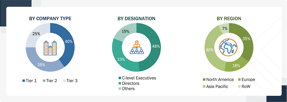
Note: The three tiers of companies are defined based on their total revenue in 2025: Tier 1 - revenue greater than or equal to USD 1 billion; Tier 2 - revenue between USD 100 million and USD 1 billion; and Tier 3 - revenue less than or equal to USD 100 million. Other designations include sales managers, marketing managers, and product managers.
To know about the assumptions considered for the study, download the pdf brochure
Market Size Estimation
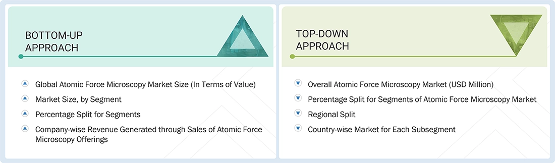
Both top-down and bottom-up approaches were used to estimate and validate the total size of the atomic force microscopy market. These methods have also been used extensively to estimate the size of various subsegments in the market. The following research methodology was used to estimate the market size:
- Major players in the atomic force microscopy market and related markets were identified through extensive secondary research.
- The industry’s value chain and market size (in terms of value) were determined through primary and secondary research processes.
- All percentage shares, splits, and segment-level breakdowns were determined using secondary sources and verified through primary sources.
Atomic Force Microscopy Market : Top-Down and Bottom-Up Approach
Data Triangulation
After arriving at the overall size of the atomic force microscopy market from the market size estimation process explained above, the total market was split into several segments and subsegments. Data triangulation and market breakdown procedures were employed, wherever applicable, to complete the overall market engineering process and arrive at the statistics for all segments and subsegments of the market. The data were triangulated by studying various factors and trends from the demand and supply sides, including offering, grade, application, and regional developments. Along with this, the market size was validated using both top-down and bottom-up approaches.
Market Definition
Atomic force microscopes (AFMs) are nanoscale imaging and measurement instruments used to examine the surface of materials and samples with very high resolution. AFMs use a sharp probe to scan the sample surface and generate detailed information about its topography, surface roughness, and other physical characteristics at the nanoscale. Atomic force microscopes are used for applications such as surface imaging, roughness measurement, defect identification, and material characterization across semiconductor and electronics, materials science and nanotechnology, chemical and polymer research, life sciences, and industrial applications. AFM systems can be used with different probes, measurement modes, and software depending on the type of sample and the specific measurement requirements.
Atomic force microscopes are particularly useful for applications that require detailed analysis of surfaces and nanoscale structures, including semiconductor wafers and devices, thin films, nanomaterials, polymers, and biological samples. They support research, product development, process monitoring, quality control, and failure analysis by providing detailed information about sample surfaces and material characteristics. A typical AFM system consists of the microscope, a probe, and software for controlling measurements and analyzing the collected data. The configuration and capabilities of AFM systems vary depending on the application, sample type, required resolution, and measurement requirements.
Key Stakeholders
- Pharmaceutical and biotechnology industries
- Semiconductor and materials industries
- Academic and research institutes
- Pathological laboratories
- Hospitals
- Medical device suppliers
- Market research and consulting firms
Report Objectives
- To describe and forecast the atomic force microscopy market size, by offering, grade, and application, in terms of value
- To describe and forecast the market for various segments across four main regions, namely North America, Europe, Asia Pacific, and RoW, in terms of value
- To strategically analyze micromarkets with regard to individual growth trends, prospects, and contribution to the overall market
- To provide detailed information regarding drivers, restraints, opportunities, and challenges influencing the market growth
- To analyze opportunities for stakeholders by identifying high-growth segments in the market
- To provide a detailed overview of the atomic force microscopy value chain
- To strategically analyze key technologies, trends impacting customers, ecosystem, regulatory landscape, patent landscape, Porter’s Five Forces, and case studies pertaining to the market
- To strategically profile key players in the atomic force microscopy market and comprehensively analyze their market share and core competencies
- To analyze competitive developments, such as partnerships, acquisitions, expansions, collaborations, agreements, and product launches in the market
Available customizations:
With the given market data, MarketsandMarkets offers customizations according to the company’s specific needs. The following customization options are available for the report:
Company Information
-
Detailed analysis and profiling of additional market players (up to 5)
Get the Full Atomic Force Microscopy Market Report
Full forecast, segment splits, and company analysis for all Atomic Force Microscopy Market.
- US Atomic Force Microscopy Market
- Canada Atomic Force Microscopy Market
- Mexico Atomic Force Microscopy Market
- Germany Atomic Force Microscopy Market
- UK Atomic Force Microscopy Market
- France Atomic Force Microscopy Market
- Italy Atomic Force Microscopy Market
- Spain Atomic Force Microscopy Market
- Netherlands Atomic Force Microscopy Market
- Russia Atomic Force Microscopy Market
- Switzerland Atomic Force Microscopy Market
- China Atomic Force Microscopy Market
- Japan Atomic Force Microscopy Market
- South Korea Atomic Force Microscopy Market
- Taiwan Atomic Force Microscopy Market
- Australia Atomic Force Microscopy Market
- Singapore Atomic Force Microscopy Market
- Malaysia Atomic Force Microscopy Market
- Thailand Atomic Force Microscopy Market
- Rest Of Europe Atomic Force Microscopy Market
- Rest Of Asia Pacific Atomic Force Microscopy Market
Need a Tailored Report?
Customize this report to your needs
Get 10% FREE Customization
Customize This Report