
South Korea Interposer and Fan-out Wafer Level Packaging Market (2024-2029)

The South Korea Interposer and Fan-out Wafer Level Packaging Market was valued at $3858.4 Million in 2024 and projected to reach to $6832.4 Million by 2029, representing a compound annual growth rate of 12.1%. South Korea's interposer and fan-out wafer level packaging market is positioned for accelerated growth through 2029, driven by the country's world-leading semiconductor manufacturing base and increasing demand for advanced packaging in memory, logic, and specialized chip applications.


| Market Size in | USD 26.32 MN |
| Market Forecast in | |
| CAGR | |
| Forecast Period | |
| Units Considered | Value (USD MN) |
South Korea Interposer and Fan-out Wafer Level Packaging Market Trends and Insights
- South Korea's semiconductor manufacturing ecosystem, anchored by leading chipmakers and advanced foundries, is driving demand for high-density interconnect solutions essential for next-generation processors and memory devices.
- The market in South Korea benefits from strong domestic R&D capabilities and strategic investments in advanced packaging technologies that support AI, 5G, and high-performance computing applications. During the 2024-2029 forecast period, South Korea is positioned as a critical hub for interposer and fan-out WLP innovation, with a compound annual growth rate of 12.1%.
- South Korea's competitive advantage stems from its established semiconductor supply chain, skilled workforce, and proximity to major electronics manufacturers.
- The expansion reflects South Korea's commitment to maintaining technological leadership in packaging solutions, which are increasingly vital for reducing form factors and improving thermal management in consumer electronics, data centers, and automotive applications..
Key Market Statistics
- CAGR (2024-2029) 12.1% CAGR
- Market Size, 2024 ~USD 3858.4 Million
- Forecast, 2029 ~USD 6832.4 Million
- Country South Korea
South Korea Interposer and Fan-out Wafer Level Packaging Market Overview
Samsung and SK Hynix Leadership :
South Korea's dominance in memory chip manufacturing drives substantial demand for advanced interposer and fan-out wafer level packaging solutions, with Samsung and SK Hynix investing heavily in next-generation packaging technologies.
High-Density Interconnect Adoption :
South Korean chipmakers are rapidly adopting fan-out wafer level packaging for HBM, chiplets, and advanced processors, enabling higher performance and reduced form factors critical for AI and data center applications.
Foundry Ecosystem Expansion :
Advanced foundries in South Korea are expanding capacity for interposer-based solutions, supporting both domestic semiconductor manufacturers and international clients seeking cutting-edge packaging capabilities.
Government Support and Investment :
South Korean government initiatives and substantial R&D investments in semiconductor manufacturing infrastructure are accelerating the adoption of advanced packaging technologies across the nation's chipmaking ecosystem.
South Korea Interposer and Fan-out Wafer Level Packaging Market Dynamics
- The market's 12.1% CAGR reflects strong momentum from major chipmakers transitioning to chiplet architectures and high-bandwidth memory solutions.
- South Korea's strategic focus on semiconductor self-sufficiency, coupled with investments in packaging innovation, will sustain competitive advantages.
- The convergence of AI chip demand, 5G/6G infrastructure requirements, and automotive electrification will further propel adoption of fan-out and interposer technologies throughout the forecast period..
Market Ecosystem
Related Ecosystem
Semiconductor Materials And Components
- Sensors
- Gallium Nitride (GaN)
- Digital Signal Processor (DSP)
- Natural Language Processing (NLP)
- Silicon Carbide
- Texas Instruments Incorporated
- Samsung
- APPLIED MATERIALS, INC.
- Stmicroelectronics
- Lenovo
Key Takeaways
- South Korea's interposer and fan-out WLP market will grow from USD 3,858.4 million (2024) to USD 6,832.4 million (2029) at a 12.1% CAGR.
- South Korea's advanced semiconductor manufacturing base and R&D infrastructure position it as a regional leader in high-density packaging innovation.
- South Korea's market growth is driven by demand from AI, 5G, and high-performance computing sectors requiring advanced interconnect solutions.
- South Korea's established supply chain and skilled workforce provide competitive advantages in developing next-generation fan-out and interposer technologies.
Interposer and Fan-out Wafer Level Packaging Market Report Scope
| Report Metric | Details |
|---|---|
| Base Year | 2024 |
| Fastest Growing Segment | 3D (Packaging Type) |
| Forecast Period | 2024-2029 |
| Growth Rate | CAGR of 12.3% from 2024 to 2029 |
| Largest Segment | INTERPOSERS (Packaging Component And Design) |
| Market Size Base Year (Billions) | ~USD 35.55 (2024) |
| Revenue Forecast (Billions) | ~USD 63.5 (2029) |
| Segments Covered | Packaging Component And Design, Packaging Type, Packaging Component, End-User Industry, Device Type |
South Korea Interposer and Fan-out Wafer Level Packaging Market Report Segmentation
5 segment dimensions are covered across the global market.
By Packaging Component And Design
- Fowlp
- Interposers
By Packaging Type
- 2.5D
- 3D
By Packaging Component
- Ceramic
- Glass
- Organic
- Other Interposers
- Silicon
By End-User Industry
- Aerospace
- Automotive
- Communications
- Consumer Electronics
- Healthcare
- Manufacturing
By Device Type
- Imaging & Optoelectronics
- Leds
- Logic Ics
- Memory Devices
- MEMS/Sensors
- Other Device Types
Target Audience
- Semiconductor Equipment Manufacturers : Equipment suppliers need South Korea-specific market data to develop targeted sales strategies, understand customer requirements, and plan manufacturing capacity for Korean chipmakers.
- Packaging Material Suppliers : Material vendors require detailed insights into South Korean demand patterns, preferred specifications, and supplier relationships to secure contracts with leading chipmakers and foundries.
- Chipmakers and Foundries : Korean and international semiconductor manufacturers need competitive benchmarking data and technology trends to guide packaging technology investments and product development roadmaps.
- Investment and Private Equity Firms : Investors evaluating opportunities in South Korea's semiconductor sector require market sizing, growth projections, and competitive landscape analysis to assess portfolio companies and acquisition targets.
- Strategic Consultants and Analysts : Consulting firms and research organizations need authoritative South Korea market data to support client advisory services, competitive analysis, and strategic planning engagements.
Reasons to Buy this Report
- Competitive Intelligence on Korean Leaders : Gain detailed insights into Samsung, SK Hynix, and other South Korean chipmakers' packaging strategies, capacity expansions, and technology roadmaps to benchmark against competitors.
- Market Entry and Expansion Strategy : Understand South Korea's regulatory environment, supply chain dynamics, and partnership opportunities essential for equipment suppliers and material vendors targeting the Korean semiconductor ecosystem.
- Technology Trend Analysis : Access comprehensive data on chiplet adoption rates, HBM integration trends, and fan-out packaging innovations specific to South Korean manufacturers and their product portfolios.
- Investment and M&A Opportunities : Identify high-growth segments, emerging players, and consolidation trends within South Korea's packaging sector to inform strategic investment and acquisition decisions.
- Demand Forecasting by Application : Leverage South Korea-specific projections for memory, logic, and specialty chip packaging to optimize production planning, inventory management, and resource allocation.
Frequently asked questions
What is the current market size of interposer and fan-out WLP in South Korea?
South Korea's interposer and fan-out wafer level packaging market was valued at USD 3,858.4 million in 2024.
What is the projected market size for South Korea by 2029?
South Korea's market is forecast to reach USD 6,832.4 million by 2029, representing significant expansion over the five-year period.
What is the CAGR for South Korea's interposer and fan-out WLP market?
South Korea's market is expected to grow at a compound annual growth rate of 12.1% from 2024 to 2029.
Which industries are driving demand in South Korea's packaging market?
South Korea's market is primarily driven by demand from AI, 5G telecommunications, high-performance computing, consumer electronics, and automotive sectors.
Why is South Korea a key market for interposer and fan-out WLP technologies?
South Korea's advanced semiconductor manufacturing ecosystem, strong R&D capabilities, established supply chains, and leading chipmakers make it a critical hub for packaging innovation and production.
RESEARCH METHODOLOGY
The study involved four major activities in estimating the current size of the interposer and fan-out wafer level packaging (FOWLP) market. Exhaustive secondary research was done to collect information on the market, peer, and parent markets. The next step was to validate these findings, assumptions, and sizing with industry experts across the value chain through primary research. Both top-down and bottom-up approaches were employed to estimate the complete market size. After that, market breakdown and data triangulation were used to estimate the market size of segments and subsegments.
Secondary Research
Various secondary sources have been referred to in the secondary research process for identifying and collecting information important for this study. The secondary sources include annual reports, press releases, and investor presentations of companies; white papers; journals and certified publications; and articles from recognized authors, websites, directories, and databases. Secondary research has been conducted to obtain key information about the industry’s supply chain, the market’s value chain, the total pool of key players, market segmentation according to the industry trends (to the bottom-most level), regional markets, and key developments from market- and technology-oriented perspectives. The secondary data has been collected and analyzed to determine the overall market size, further validated by primary research.
List of major secondary sources
|
Sources |
Web Link |
|
Chinese American Semiconductor Professional Association |
http://www.caspa.com/ |
|
Global Semiconductor Alliance |
https://www.gsaglobal.org/ |
|
Semiconductor Equipment Association of Japan (SEAJ) |
https://www.seaj.or.jp/english/ |
|
China Semiconductor Industry Association |
http://www.csia.net.cn/wsc/ |
|
SEMI |
https://www.semi.org/en |
Primary Research
Extensive primary research was conducted after gaining knowledge about the current scenario of the interposer and FOWLP market through secondary research. Several primary interviews were conducted with experts from both the demand and supply sides across four major regions—North America, Europe, Asia Pacific and RoW. This primary data was collected through questionnaires, emails, and telephonic interviews.
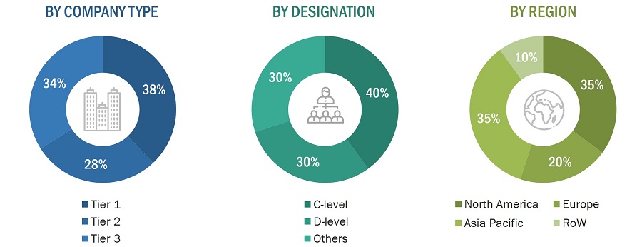
To know about the assumptions considered for the study, download the pdf brochure
Market Size Estimation
In the complete market engineering process, both top-down and bottom-up approaches have been used, along with several data triangulation methods, to perform market estimation and forecasting for the overall market segments and subsegments listed in this report. Key players in the market have been identified through secondary research, and their market shares in the respective regions have been determined through primary and secondary research. This entire procedure includes the study of annual and financial reports of the top market players and extensive interviews for key insights (quantitative and qualitative) with industry experts (CEOs, VPs, directors, and marketing executives).
All percentage shares, splits, and breakdowns have been determined using secondary sources and verified through primary sources. All the parameters affecting the markets covered in this research study have been accounted for, viewed in detail, verified through primary research, and analyzed to obtain the final quantitative and qualitative data. This data has been consolidated and supplemented with detailed inputs and analysis from MarketsandMarkets and presented in this report. The following figure represents this study’s overall market size estimation process.
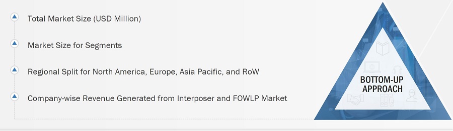
Bottom-Up Approach
The bottom-up approach was used to arrive at the overall size of the interposer and FOWLP market from the revenues of the key players and their shares in the market. The overall market size was calculated based on the revenues of the key players identified in the market.
- Identifying entities in the interposer and FOWLP value chain influencing the entire semiconductor packaging industry
- Analyzing each entity along with related major companies identifying technology providers for the implementation of offerings and services
- Estimating the market for these interposers and FOWLP end users
- Tracking ongoing and upcoming implementation of interposer and FOWLP developments by various companies and forecasting the market based on these developments and other critical parameters
- Arriving at the market size by analyzing interposer and FOWLP companies based on their countries and then combining it to get the market estimate by region
- Verifying estimates and crosschecking them by a discussion with key opinion leaders, which include CXOs, directors, and operation managers
Top-Down Approach
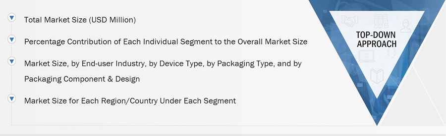
In the top-down approach, the overall market size has been used to estimate the size of individual markets (mentioned in the market segmentation) through percentage splits from secondary and primary research.
The most appropriate immediate parent market size has been used to implement the top-down approach to calculate the market size of specific segments. The top-down approach has been implemented for the data extracted from the secondary research to validate the market size obtained.
Each company’s market share has been estimated to verify the revenue shares used earlier in the top-down approach. This study has determined and confirmed the overall parent market and individual market sizes by the data triangulation method and data validation through primaries. The data triangulation method in this study is explained in the next section.
- Focusing initially on topline investments by market players in the semiconductor packaging ecosystem
- Calculating the market size based on the revenue generated by market players through the sales of interposer and fan-out and wafer level packaging.
- Mapping the use of interposer and FOWLP in different offerings.
- Building and developing the information related to the revenue generated by market players through key products
- Estimating the geographic split using secondary sources considering factors, such as the number of players in a specific country and region, the role of major players in the development of innovative products, and adoption and penetration rates in a particular country for various segments.
Data Triangulation
After arriving at the overall market size from the estimation process explained above, the overall market has been split into several segments and subsegments. The data triangulation procedure has been employed wherever applicable to complete the overall market engineering process and arrive at the exact statistics for all segments and subsegments. The data has been triangulated by studying various factors and trends from both the demand and supply sides. Additionally, the market size has been validated using top-down and bottom-up approaches.
Market Definition
Interposer and fan-out wafer level packaging (FOWLP) are key technologies in the semiconductor packaging industry. An interposer serves as an intermediary substrate, allowing the integration of many semiconductor dies into a single package via a network of interconnects and perhaps passive components.
FOWLP is a packaging technology that redistributes external connections from a thinned semiconductor die to the package substrate, resulting in a more compact design with better electrical performance. This market is driven by the growing demand for smaller, more powerful, and energy-efficient electronic devices across various industries.
Key Stakeholders
- Suppliers of Raw Materials and Manufacturing Equipment
- Providers and Manufacturers of Components
- Providers of Software Solutions
- Manufacturers and Providers of Semiconductor Devices
- Original Equipment Manufacturers (OEMs)
- ODM and OEM Technology Solution Providers
- Suppliers and Distributors of Semiconductor Manufacturing Devices
- System Integrators
- Assembly, Testing, and Packaging Vendors
- Market Research and Consulting Firms
- Associations, Organizations, Forums, and Alliances Related to the Semiconductor Packaging
- Technology Investors
- Governments, Regulatory Bodies, and Financial Institutions
- Venture Capitalists, Private Equity Firms, and Startups
- End-user Industries
Report Objectives
- To describe and forecast the interposer and fan-out wafer level packaging (FOWLP) market, in terms of value, based on packaging component & design, packaging type, device type and end-user industry.
- To forecast the market size, in terms of value, for various segments concerning four regions: North America, Europe, Asia Pacific, and the Rest of the World.
- To provide detailed information regarding the major factors influencing the market growth (drivers, restraints, opportunities, and challenges).
- To strategically analyze micromarkets1 for individual growth trends, prospects, and contributions to the total market.
- To analyze market opportunities for stakeholders by identifying well-developed segments of the interposer and fan-out wafer level packaging (FOWLP) market.
- To provide a detailed overview of the market's value chain and analyze market trends with Porter’s five forces analytical framework.
- To strategically profile the key players and comprehensively analyze their market position regarding ranking and core competencies2, along with detailing the competitive landscape for market leaders.
- To analyze strategic developments, such as product launches, related developments, acquisitions, expansions, and agreements in the interposer and fan-out wafer level packaging (FOWLP) market.
- To track and analyze competitive developments, such as partnerships, collaborations, agreements, joint ventures, mergers and acquisitions, expansions, product launches, and other developments in the market.
Customization Options
With the given market data, MarketsandMarkets offers customizations according to the company’s specific needs. The following customization options are available for the report:
Company Information
- Detailed analysis and profiling of additional market players (up to five)
Geographic Analysis
- Further breakdown of regions into respective countries
Get the Full Interposer and Fan-out Wafer Level Packaging Market Report
Full forecast, segment splits, and company analysis for all Interposer and Fan-out Wafer Level Packaging Market.
- US Interposer and Fan-out Wafer Level Packaging Market
- Canada Interposer and Fan-out Wafer Level Packaging Market
- Mexico Interposer and Fan-out Wafer Level Packaging Market
- Germany Interposer and Fan-out Wafer Level Packaging Market
- UK Interposer and Fan-out Wafer Level Packaging Market
- France Interposer and Fan-out Wafer Level Packaging Market
- Rest Of Europe Interposer and Fan-out Wafer Level Packaging Market
- China Interposer and Fan-out Wafer Level Packaging Market
- Japan Interposer and Fan-out Wafer Level Packaging Market
- Rest Of Asia Pacific Interposer and Fan-out Wafer Level Packaging Market
Need a Tailored Report?
Customize this report to your needs
Get 10% FREE Customization
Customize This Report